|
データシートサーチシステム |
|
|
データシートサーチシステム |
|
ADE7569 データシート(PDF) 94 Page - Analog Devices |
|
|
|||||||||||||||||||||||||||||
ADE7569 データシート(HTML) 94 Page - Analog Devices |
|
|
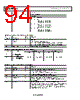
94 / 148 page  ADE75xx/ADE71xx Preliminary Technical Data Rev. PrE | Page 94 of 148 1 1/3 LCD Multiplex level LMUX[1:0] 0 0 Reserved 0 1 2x FP27/COM3 is used as FP27 FP28/COM2 is used as FP28 1 0 3x FP27/COM3 is used as FP27 FP28/COM2 is used as COM2 1-0 LMUX[1:0] 0 1 1 4x FP27/COM3 is used as COM3 FP28/COM2 is used as COM2 Table 75. LCD Configuration X SFR (LCDCONX, 0x9C) Bit Location Bit Mnemonic Default Value Description 7 Reserved 0 Reserved External Resistor Ladder selection bit. 0 External resistor ladder is disabled. Charge pump is enabled. 6 EXTRES 0 1 External resistor ladder is enabled. Charge pump is disabled. 5-0 BIASLVL[5:0] 0 Bias Level Selection bits. See Table 76. Table 76. LCD bias voltage when contrast control is enabled 1/2 Bias 1/3 Bias BLVL[5] VA (V) VB VC VB VC 0 [] 31 0 : 4 BLVL V ref × 1 [] ⎟ ⎠ ⎞ ⎜ ⎝ ⎛ + × 31 0 : 4 1 BLVL V ref VB = VA VC = 2 x VA VB = 2 x VA VC = 3 x VA Table 77. LCD Configuration Y SFR (LCDCONY, 0xB1) Bit Location Bit Mnemonic Default Value Description 7 Reserved 0 This bit should be kept cleared for proper operation 6 INV_LVL 0 Frame Inversion Mode Enable bit If this bit is set, frames are inverted every other frame If this bit is cleared, frames are not inverted 5-2 Reserved 0 These bits should be kept cleared for proper operation 1 UPDATEOVER 0 Update finished flag bit. This bit is updated by LCD driver. When set, indicates that the LCD memory has been updated and a new frame has begun. 0 REFRESH 0 Refresh LCD data memory bit, this bit should be set by user. When set, the LCD driver does not use the data in the LCD data registers to update display. The LCD data registers can be updated by the 8052. When clear, the LCD driver will use the data in the LCD data registers to update display at the next frame. |
|
リンク URL |
| ALLDATASHEETはお客様のビジネスに役立ちますか? [ DONATE ] |
Alldatasheetは | 広告 | お問い合わせ | プライバシーポリシー | データシートへのリンク | リンク交換 | メーカーリスト All Rights Reserved©Alldatasheet.com |
| Russian : Alldatasheetru.com | Korean : Alldatasheet.co.kr | Spanish : Alldatasheet.es | French : Alldatasheet.fr | Italian : Alldatasheetit.com Portuguese : Alldatasheetpt.com | Polish : Alldatasheet.pl | Vietnamese : Alldatasheet.vn Indian : Alldatasheet.in | Mexican : Alldatasheet.com.mx | British : Alldatasheet.co.uk | New Zealand : Alldatasheet.co.nz |
|
Family Site : ic2ic.com |
icmetro.com |
 Japanese ▼
 English
 Chinese
 German
 Japanese
 Russian
 Korean
 Spanish
 French
 Italian
 Portuguese
 Polish
 Vietnamese
 Indian
 Mexican
 British
 New Zealand