|
データシートサーチシステム |
|
|
データシートサーチシステム |
|
WM8733 データシート(PDF) 3 Page - Wolfson Microelectronics plc |
|
|
|||||||||||||||||||||||||||||
WM8733 データシート(HTML) 3 Page - Wolfson Microelectronics plc |
|
|
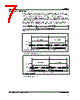
3 / 11 page  Product Preview WM8733 WOLFSON MICROELECTRONICS LTD PP Rev 1.3 July 2000 3 ELECTRICAL CHARACTERISTICS Test Characteristics VDD = 5V, GND = 0V, TA = +25 oC, fs = 44.1kHz, SCKI = 384fs unless otherwise stated. PARAMETER SYMBOL TEST CONDITIONS MIN TYP MAX UNIT Digital Logic Levels Input LOW level VIL 0.8 V Input HIGH level VIH 2.0 V Analogue Output Levels Output level Into 10kohm, full scale 0dB, (5V supply) 1VRMS Into 10kohm, full scale 0dB, (3V supply) 0.6 VRMS o midrail or AC coupled (5V supply) 2 10 kohms Minimum resistance load o midrail or AC coupled (3V supply) 10 kohms Maximum capacitance load 5V or 3V 100 pF Output DC level VDD/2 V Reference Levels Potential divider resistance VDD to CAP and CAP to GND 80 100 120 kohms Voltage at CAP VDD/2 DAC Circuit Specifications SNR (Note 1) Stereo mode 98 102 dB Mono mode VDD = 5V dB Stereo mode 96 100 dB Mono mode VDD = 3V dB THD (full scale) 0dB 0.03 0.01 % THD+N -60dB -35 -40 dB Frequency response 0 20,000 Hz Pass band ripple ±0.25 dB Transition band 20,000 Hz Out of band rejection -40 dB Stereo mode 100 dB Dynamic Range Mono mode dB Channel Separation 90 dB Gain mismatch channel-to-channel ±1 ±5 %FSR Audio Data Input and System Clock Timing Information BCKIN pulse cycle time tBCY 100 ns BCKIN pulse width high tBCH 50 ns BCKIN pulse width low tBCL 50 ns BCKIN rising edge to LRCIN edge tBL 30 ns LRCIN rising edge to BCKIN rising edge tLB 30 ns DIN setup time tDS 30 ns DIN hold time tDH 30 ns System clock pulse width high tSCKIH 13 ns System clock pulse width low tSCKIL 13 ns Note 1 Ratio of RMS output level with 1kHz full scale input, to the RMS output level with all zeros into the digital input, measured “A” weighted over a 20Hz to 20kHz bandwidth. Note 2 All performance measurements done with 20kHz low pass filter. Failure to use such a filter will result in higher THD+N and lower SNR and Dynamic Range readings than are found in the Electrical Characteristics. The low pass filter removes out of band noise; although it is not audible it may affect dynamic specification values. |
|
|
リンク URL |
| ALLDATASHEETはお客様のビジネスに役立ちますか? [ DONATE ] |
Alldatasheetは | 広告 | お問い合わせ | プライバシーポリシー | データシートへのリンク | リンク交換 | メーカーリスト All Rights Reserved©Alldatasheet.com |
| Russian : Alldatasheetru.com | Korean : Alldatasheet.co.kr | Spanish : Alldatasheet.es | French : Alldatasheet.fr | Italian : Alldatasheetit.com Portuguese : Alldatasheetpt.com | Polish : Alldatasheet.pl | Vietnamese : Alldatasheet.vn Indian : Alldatasheet.in | Mexican : Alldatasheet.com.mx | British : Alldatasheet.co.uk | New Zealand : Alldatasheet.co.nz |
|
Family Site : ic2ic.com |
icmetro.com |
 Japanese ▼
 English
 Chinese
 German
 Japanese
 Russian
 Korean
 Spanish
 French
 Italian
 Portuguese
 Polish
 Vietnamese
 Indian
 Mexican
 British
 New Zealand