|
データシートサーチシステム |
|
|
データシートサーチシステム |
|
MIC25400 データシート(PDF) 3 Page - Micrel Semiconductor |
|
|
|||||||||||||||||||||||||||||
MIC25400 データシート(HTML) 3 Page - Micrel Semiconductor |
|
|
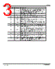
3 / 27 page  Micrel, Inc. MIC25400 January 2011 3 M9999-020111-C Pin Number Pin Name Pin Description 13 EN/DLY2 Enable/Delay 2 (Input): This pin can be used to disable VOUT2. When used to disable VOUT2, this pin must be pulled down to ground in less than 1µs for proper operation. It is also used for soft-start of the output. Soft start capacitor range is 4.7nf to 22nf. See Functional Description section for additional information. 14 PG2 Power Good 2 (Output) Open drain. Device is in the OFF state. i.e., high when output is within 90% of regulation 15 CS2 Current Sense 2 (Input) Place a resistor from SW2 to this pin to program the current limit point from 0.5A to 2.7A 16 PGND2 Power Ground 2 (Input) 17 LSD2 Low-side Drive 2 (Output): External low-side N-Channel MOSFET driver. Use 4.5V rated MOSFETs. 18 BST2 Boost 2 (Input): Provides voltage for high-side internal MOSFET for Channel 2. Connect a 0.01µF capacitor from SW2 to BST2 pin and a diode-to-PVDD. 19 SW2 Switch Node 2 (Output): Source of internal high-side power MOSFET. 20 VIND2 Supply voltage (Input): For the drain of internal high-side power MOSFET 4.5V to 13.2V. 21 PVDD 5V Internal Linear Regulator (Output): PVDD is the external MOSFET gate drive for LSD1 and LSD2 and an internal supply bus for the IC. Connect to an external 1µF bypass capacitor. When VIN is <6V, this regulator operates in drop-out mode. Connect VDD to VIN when VIN <6V. 22 VIN Supply voltage (Input): For the internal 5V linear regulator. 4.5V to 13.2V. 23 VIND1 Supply voltage (Input): For the drain of internal high-side power MOSFET 4.5V to 13.2V. 24 SW1 Switch Node 1 (Output): Source of internal high-side power MOSFET. EP GND Exposed thermal pad for package only. Connect to ground. Must make a full connection to the ground plane to maximize thermal performance of the package. |
|
|
リンク URL |
| ALLDATASHEETはお客様のビジネスに役立ちますか? [ DONATE ] |
Alldatasheetは | 広告 | お問い合わせ | プライバシーポリシー | データシートへのリンク | リンク交換 | メーカーリスト All Rights Reserved©Alldatasheet.com |
| Russian : Alldatasheetru.com | Korean : Alldatasheet.co.kr | Spanish : Alldatasheet.es | French : Alldatasheet.fr | Italian : Alldatasheetit.com Portuguese : Alldatasheetpt.com | Polish : Alldatasheet.pl | Vietnamese : Alldatasheet.vn Indian : Alldatasheet.in | Mexican : Alldatasheet.com.mx | British : Alldatasheet.co.uk | New Zealand : Alldatasheet.co.nz |
|
Family Site : ic2ic.com |
icmetro.com |
 Japanese ▼
 English
 Chinese
 German
 Japanese
 Russian
 Korean
 Spanish
 French
 Italian
 Portuguese
 Polish
 Vietnamese
 Indian
 Mexican
 British
 New Zealand