|
データシートサーチシステム |
|
|
データシートサーチシステム |
|
AD780 データシート(PDF) 6 Page - Analog Devices |
|
|
|||||||||||||||||||||||||||||
AD780 データシート(HTML) 6 Page - Analog Devices |
|
|
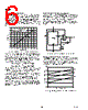
6 / 10 page  AD780 REV. B –6– TEMPERATURE OUTPUT PIN The AD780 provides a “TEMP” output (Pin 3) that varies linearly with temperature. This output can be used to monitor changes in system ambient temperature and to initiate calibration of the system if desired. The voltage VTEMP is 560 mV at 25 °C, and the temperature coefficient is approximately 2 mV/ °C. Figure 8 shows the typical VTEMP characteristic curve over tem- perature taken at the output of the op amp with a noninverting gain of five. 4.25 2.00 150 2.50 2.25 –50 –75 2.75 3.00 3.25 3.50 3.75 4.00 125 100 75 50 25 0 –25 TEMPERATURE – C CIRCUIT CALIBRATED AT 25 C REFER TO FIGURE 9 10mV PER C Figure 8. Temperature Pin Transfer Characteristic Since the TEMP voltage is acquired from the bandgap core cir- cuit, current pulled from this pin will have a significant effect on VOUT. Care must be taken to buffer the TEMP output with a suitable op amp, e.g., an OP07, AD820 or AD711 (all of which would result in less than a 100 µV change in VOUT). The rela- tionship between ITEMP and VOUT is as follows: ∆V OUT = 5.8 mV/ µA × I TEMP (2.5 V range) or ∆V OUT = 6.9 mV/ µA × I TEMP (3.0 V range) Notice how sensitive the current dependent factor on VOUT is. A large amount of current, even in tens of microamp, drawn from TEMP pin can cause VOUT and TEMP Output to fail. The choice of C1 and C2 was dictated primarily by the need for a relatively flat response that rolled off early in the high frequency noise at the output. But there is considerable margin in the choice of these capacitors. For example, the user can actually put a huge C2 on the TEMP pin with none on the output pin. However, one must either put very little or a lot of capacitance at the TEMP pin. Intermediate values of capacitance can sometimes cause oscillation. In any case, the user should follow the recom- mendation in Figure 3. TEMPERATURE TRANSDUCER CIRCUIT The circuit shown in Figure 9 is a temperature transducer which a amplifies the TEMP output voltage by a gain of a little over 5 to provide a wider full scale output range. The trimpot can be used to adjust the output so it varies exactly by 10 mV/ °C. To minimize resistance changes with temperature, resistors with low temperature coefficients, such as metal film resistors should be used. +5V VIN TEMP GND AD820 6.04k (1%) 1.27k (1%) 200 RF RB RBP 10mV/ C 1 F AD780 Figure 9. Differential Temperature Transducer SUPPLY CURRENT OVER TEMPERATURE The AD780’s quiescent current will vary slightly over tempera- ture and input supply range. The test limit is 1 mA over the in- dustrial and 1.3 mA over the military temperature range. Typical performance with input voltage and temperature varia- tion is shown in Figure 10 following. 0.85 0.60 36 0.75 0.65 0.70 4 0.80 INPUT VOLTAGE – Volts –55 C 125 C 25 C Figure 10. Typical Supply Current over Temperature |
|
|
リンク URL |
| ALLDATASHEETはお客様のビジネスに役立ちますか? [ DONATE ] |
Alldatasheetは | 広告 | お問い合わせ | プライバシーポリシー | データシートへのリンク | リンク交換 | メーカーリスト All Rights Reserved©Alldatasheet.com |
| Russian : Alldatasheetru.com | Korean : Alldatasheet.co.kr | Spanish : Alldatasheet.es | French : Alldatasheet.fr | Italian : Alldatasheetit.com Portuguese : Alldatasheetpt.com | Polish : Alldatasheet.pl | Vietnamese : Alldatasheet.vn Indian : Alldatasheet.in | Mexican : Alldatasheet.com.mx | British : Alldatasheet.co.uk | New Zealand : Alldatasheet.co.nz |
|
Family Site : ic2ic.com |
icmetro.com |
 Japanese ▼
 English
 Chinese
 German
 Japanese
 Russian
 Korean
 Spanish
 French
 Italian
 Portuguese
 Polish
 Vietnamese
 Indian
 Mexican
 British
 New Zealand