|
データシートサーチシステム |
|
|
データシートサーチシステム |
|
AD780 データシート(PDF) 3 Page - Analog Devices |
|
|
|||||||||||||||||||||||||||||
AD780 データシート(HTML) 3 Page - Analog Devices |
|
|
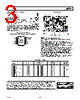
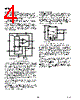
3 / 10 page  AD780 REV. B –3– ORDERING GUIDE Initial Temperature Temperature Package Model Error Range Coefficient Options AD780AN 5.0 mV –40 °C to +85°C 7 ppm/ °C Plastic Dip AD780AR 5.0 mV –40 °C to +85°C 7 ppm/ °C SOIC AD780AR-REEL7 5.0 mV –40 °C to +85°C 7 ppm/ °C SOIC AD780BN 1.0 mV –40 °C to +85°C 3 ppm/ °C Plastic Dip AD780BR 1.0 mV –40 °C to +85°C 3 ppm/ °C SOIC AD780BR-REEL 1.0 mV –40 °C to +85°C 3 ppm/ °C SOIC AD780BR-REEL7 1.0 mV –40 °C to +85°C 3 ppm/ °C SOIC AD780CR 1.5 mV –40 °C to +85°C 7 ppm/ °C SOIC AD780CR-REEL7 1.5 mV –40 °C to +85°C 7 ppm/ °C SOIC ABSOLUTE MAXIMUM RATINGS* VIN to Ground . . . . . . . . . . . . . . . . . . . . . . . . . . . . . . . . . . 36 V Trim Pin to Ground . . . . . . . . . . . . . . . . . . . . . . . . . . . . . 36 V Temp Pin to Ground . . . . . . . . . . . . . . . . . . . . . . . . . . . . . 36 V Power Dissipation (25 °C) . . . . . . . . . . . . . . . . . . . . . . 500 mW Storage Temperature . . . . . . . . . . . . . . . . . . . –65 °C to +150°C Lead Temperature (Soldering, 10 sec) . . . . . . . . . . . . . 300 °C Output Protection: Output safe for indefinite short to ground and momentary short to VIN. ESD Classification . . . . . . . . . . . . . . . . . . . . . Class 1 (1000 V) *Stresses above those listed under Absolute Maximum Ratings may cause perma- nent damage to the device. This is a stress rating only; functional operation of the device at these or any conditions above those indicated in the operational specifi- cation is not implied. Exposure to absolute maximum specifications for extended periods may affect device reliability. PIN CONFIGURATION 8-Lead Plastic DIP, SOIC and Cerdip Packages 1 2 3 4 8 7 6 5 TOP VIEW (Not to Scale) AD780 2.5/3.0V SELECT (NC OR GND) NC VOUT TRIM NC +VIN TEMP GND NC = NO CONNECT DIE LAYOUT NOTES Both VOUT pads should be connected to the output Die Thickness: The standard thickness of Analog Devices Bipolar dice is 24 mils ±2 mils. Die Dimensions: The dimensions given have a tolerance of ± 2 mils. Backing: The standard backside surface is silicon (not plated). Analog Devices does not recommend gold-backed dice for most applications. Edges: A diamond saw is used to separate wafers into dice thus providing per- pendicular edges half-way through the die. In contrast to scribed dice, this technique provides a more uniform die shape and size. The perpendicular edges facilitate handling (such as tweezer pick-up) while the uniform shape and size simplifies substrate design and die attach. Top Surface: The standard top surface of the die is covered by a layer of glassivation. All areas are covered except bonding pads and scribe lines. Surface Metalization: The metalization to Analog Devices bipolar dice is alu- minum. Minimum thickness is 10,000Å. Bonding Pads: All bonding pads have a minimum size of 4.0 mils by 6.0 mils. The passivation windows have a 3.6 mils by 5.6 mils minimum size. CAUTION ESD (electrostatic discharge) sensitive device. Electrostatic charges as high as 4000 V readily accumulate on the human body and test equipment and can discharge without detection. Although the AD780 features proprietary ESD protection circuitry, permanent damage may occur on devices subjected to high-energy electrostatic discharges. Therefore, proper ESD precautions are recommended to avoid performance degradation or loss of functionality. WARNING! ESD SENSITIVE DEVICE |
|
|
リンク URL |
| ALLDATASHEETはお客様のビジネスに役立ちますか? [ DONATE ] |
Alldatasheetは | 広告 | お問い合わせ | プライバシーポリシー | データシートへのリンク | リンク交換 | メーカーリスト All Rights Reserved©Alldatasheet.com |
| Russian : Alldatasheetru.com | Korean : Alldatasheet.co.kr | Spanish : Alldatasheet.es | French : Alldatasheet.fr | Italian : Alldatasheetit.com Portuguese : Alldatasheetpt.com | Polish : Alldatasheet.pl | Vietnamese : Alldatasheet.vn Indian : Alldatasheet.in | Mexican : Alldatasheet.com.mx | British : Alldatasheet.co.uk | New Zealand : Alldatasheet.co.nz |
|
Family Site : ic2ic.com |
icmetro.com |
 Japanese ▼
 English
 Chinese
 German
 Japanese
 Russian
 Korean
 Spanish
 French
 Italian
 Portuguese
 Polish
 Vietnamese
 Indian
 Mexican
 British
 New Zealand