|
データシートサーチシステム |
|
|
データシートサーチシステム |
|
ADL5350ACPZ-R7 データシート(PDF) 20 Page - Analog Devices |
|
|
|||||||||||||||||||||||||||||
ADL5350ACPZ-R7 データシート(HTML) 20 Page - Analog Devices |
|
|
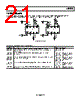
20 / 24 page  ADL5350 Rev. 0 | Page 20 of 24 Figure 63 depicts a crossover filter network approach to provide isolation between the RF and IF ports for a downconverting application. The crossover network essentially provides a high- pass filter to allow the RF signal to pass to the RF/IF node (Pin 1 and Pin 8), while presenting a low-pass filter (which is actually a band-pass filter when considering the dc blocking capacitor, CAC). This allows the difference component (fRF − fLO) to be passed to the desired IF load. RF/IF GND2 LOIN NC RF/IF NC VPOS 3.8nH 100pF C2 1.8pF L2 1.5nH CAC 100pF C1 1.2pF LO 100pF 2.2nH RF 3V IF GND1 ADL5350 12 3 4 87 6 5 L1 3.5nH 4.7µF ALL INDUCTORS ARE 0302CS SERIES FROM COILCRAFT Figure 63. 3.3 GHz to 3.8 GHz RF Downconversion Schematic When designing the RF port and IF port networks, it is important to remember that the networks share a common node (the RF/IF pins). In addition, the opposing network presents some loading impedance to the target network being designed. Classic audio crossover filter design techniques can be applied to help derive component values. However, some caution must be applied when selecting component values. At high RF frequencies, the board parasitics can significantly influence the final optimum inductor and capacitor component selections. Some empirical testing may be necessary to optimize the RF and IF port filter networks. The performance of the circuit depicted in Figure 63 is provided in Figure 64. 30 25 20 15 10 5 0 14 2 4 6 8 10 12 3300 3800 3700 3600 3500 3400 RF FREQUENCY (MHz) IIP3 IP1dB LOSS Figure 64. Measured Performance for Circuit in Figure 63 Using Low-Side LO Injection and 800 MHz IF |
|
|
リンク URL |
| ALLDATASHEETはお客様のビジネスに役立ちますか? [ DONATE ] |
Alldatasheetは | 広告 | お問い合わせ | プライバシーポリシー | データシートへのリンク | リンク交換 | メーカーリスト All Rights Reserved©Alldatasheet.com |
| Russian : Alldatasheetru.com | Korean : Alldatasheet.co.kr | Spanish : Alldatasheet.es | French : Alldatasheet.fr | Italian : Alldatasheetit.com Portuguese : Alldatasheetpt.com | Polish : Alldatasheet.pl | Vietnamese : Alldatasheet.vn Indian : Alldatasheet.in | Mexican : Alldatasheet.com.mx | British : Alldatasheet.co.uk | New Zealand : Alldatasheet.co.nz |
|
Family Site : ic2ic.com |
icmetro.com |
 Japanese ▼
 English
 Chinese
 German
 Japanese
 Russian
 Korean
 Spanish
 French
 Italian
 Portuguese
 Polish
 Vietnamese
 Indian
 Mexican
 British
 New Zealand