|
データシートサーチシステム |
|
|
データシートサーチシステム |
|
CLC420 データシート(PDF) 8 Page - National Semiconductor (TI) |
|
|
|
|||||||||||||||||||||||||||||
CLC420 データシート(HTML) 8 Page - National Semiconductor (TI) |
|
|
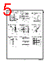
8 / 10 page  Application Division (Continued) Transimpedance amplifier circuits Low inverting, input current noise (2pA/ ) makes the CLC420 ideal for high-sensitivity transimpedance amplifier circuits for applications such as pin-diode optical receivers, and detectors in receiver IFs. However, feedback resistors 4k Ω or greater are required if feedback resistor noise current is going to be less than the input current noise contribution of the op-amp. With feedback resistors this large, shunt capacitance on the inverting input of the op-amp (from the pin-diode, etc.) will unacceptably degrade phase margin causing frequency re- sponse peaking or oscillations a small valued capacitor shunting the feedback resistor solves this problem (Note: This approach does not work for a current-feedback op-amp configured for transimpedance applications). To determine the value of this capacitor, refer to the “Transimpedance BW vs. R f and Ci” plot. For example, let’s assume an optical transimpedance re- ceiver is being developed. Total capacitance from the invert- ing input to ground, including the photodiode and strays is 5pF. A 5k Ω feedback resistor value has been determined to provide best dynamic range based on the response of the photodiode and the range of incident optical powers, etc. From the “Transimpedance BW vs. R f and Ci” plot, using C i=5pF it is determined from the two curves labeled Ci=5pF, that C f=1.5pF provides optimal compensation (no more than 0.5dB frequency response peaking) and a −3dB bandwidth of approximately 27MHz. Printed circuit layout As with any high frequency device, a good PCB layout will enhance performance. Ground plane construction and good power supply bypassing close to the package are critical to achieving full performance. The amplifier is sensitive to stray capacitance to ground at the output and inverting input: Node connections should be small with minimal coupling to the ground plane. Parasitic or load capacitance directly on the output (pin 6) will introduce additional phase shift in the loop degrading the loop phase margin and leading to frequency response peak- ing. A small series resistor before this capacitance, if present, effectively decouples this effect. The graphs on the preceding page, “ Settling Time vs. C L”, illustrates the re- quired resistor value and resulting performance vs. capaci- tance. Evaluation PC boards (part no. 730013 for through-hole and CLC730027 for SOIC) are available for the CLC420. www.national.com 8 |
|
|
リンク URL |
| ALLDATASHEETはお客様のビジネスに役立ちますか? [ DONATE ] |
Alldatasheetは | 広告 | お問い合わせ | プライバシーポリシー | データシートへのリンク | リンク交換 | メーカーリスト All Rights Reserved©Alldatasheet.com |
| Russian : Alldatasheetru.com | Korean : Alldatasheet.co.kr | Spanish : Alldatasheet.es | French : Alldatasheet.fr | Italian : Alldatasheetit.com Portuguese : Alldatasheetpt.com | Polish : Alldatasheet.pl | Vietnamese : Alldatasheet.vn Indian : Alldatasheet.in | Mexican : Alldatasheet.com.mx | British : Alldatasheet.co.uk | New Zealand : Alldatasheet.co.nz |
|
Family Site : ic2ic.com |
icmetro.com |
 Japanese ▼
 English
 Chinese
 German
 Japanese
 Russian
 Korean
 Spanish
 French
 Italian
 Portuguese
 Polish
 Vietnamese
 Indian
 Mexican
 British
 New Zealand