|
データシートサーチシステム |
|
|
データシートサーチシステム |
|
TPS65232A2 データシート(PDF) 8 Page - Texas Instruments |
|
|
|
|||||||||||||||||||||||||||||
TPS65232A2 データシート(HTML) 8 Page - Texas Instruments |
|
|
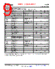
8 / 32 page  TPS65232 SLVSA42 – FEBRUARY 2010 www.ti.com RECOMMENDED OPERATING CONDITIONS over operating free-air temperature range (unless otherwise noted) MIN NOM MAX UNIT Input voltage range at VIN 10.8 12 22 V Input voltage range at VINB 4.75 6.1 Voltage range, EN_BCK1, EN_BCK2, EN_BCK3 0 3.3 V TA Ambient operating temperature 0 50 °C ELECTRICAL CHARACTERISTICS VIN = 12 V ±5%, VINB2, VINB3 = 5 V ±5%, TJ = 0°C to 150°C (unless otherwise noted) PARAMETER TEST CONDITIONS MIN TYP MAX UNIT INPUT VOLTAGE VIN Input supply voltage 10.8 12 22 V VIN rising 10.8 UVLO VIN UVLO threshold – VIN (main supply) V VIN falling 4.7 VINB rising 4.75 UVLO threshold – VINB UVLO VINB V (BUCK2/BUCK3 supply) VINB falling 4.25 INPUT CURRENT All regulators/USB switches ICCQ Input supply current 4 mA disabled BUCK ENABLE INPUTS (EN_BCK1,2,3) VEN Enable threshold 1.2 V VENHYS Enable voltage hysteresis 100 mV IPULLUP Pull-up current tEN = 0.2 ms/nF 6 mA RD Discharge resistor 1 k Ω tD Discharge time Power-up 5 ms PWM CONTROLLER (BUCK1) VOUT Output voltage range(1) 3.3 6.1 V VFB Feedback voltage –2% 0.804 2% V LDRV High and low side drive voltage No load 6 V HDRV R_ONLDRV Low side ON resistance 8 Ω R_OFFLDRV Low side OFF resistance 1 Ω R_ONHDRV High side ON resistance 20 Ω R_OFFHDRV High side OFF resistance 1 Ω d Duty cycle(2) 20 80 % AMOD Modulator gain 12 fSW Switching frequency 500 kHz Current source for setting OCP trip ITRIP TA = 25°C 10 mA point TCTRIP Temperature coefficient of ITRIP 3700 ppm/°C RTRIP Current-limit setting resistor 80 250 kW COUT Output capacitance 22(3) mF L Nominal inductance Recommended 4.7 mH BUCK2 VOUT Output voltage range(1) 0.9 3.3 V VFB Feedback voltage – 2% 0.804 2% V (1) Output voltage range is limited by the minimum and maximum duty cycle. VOUT(min) ~ d(min) x VINPUT and VOUT(max) ~ d(max) x VINPUT. (2) Performance outside these limits is not guaranteed. (3) Absolute value. User should make allowances for tolerance and variations due to component selection. 8 Submit Documentation Feedback Copyright © 2010, Texas Instruments Incorporated Product Folder Link(s): TPS65232 Not Recommended for New Designs |
|
リンク URL |
| ALLDATASHEETはお客様のビジネスに役立ちますか? [ DONATE ] |
Alldatasheetは | 広告 | お問い合わせ | プライバシーポリシー | データシートへのリンク | リンク交換 | メーカーリスト All Rights Reserved©Alldatasheet.com |
| Russian : Alldatasheetru.com | Korean : Alldatasheet.co.kr | Spanish : Alldatasheet.es | French : Alldatasheet.fr | Italian : Alldatasheetit.com Portuguese : Alldatasheetpt.com | Polish : Alldatasheet.pl | Vietnamese : Alldatasheet.vn Indian : Alldatasheet.in | Mexican : Alldatasheet.com.mx | British : Alldatasheet.co.uk | New Zealand : Alldatasheet.co.nz |
|
Family Site : ic2ic.com |
icmetro.com |
 Japanese ▼
 English
 Chinese
 German
 Japanese
 Russian
 Korean
 Spanish
 French
 Italian
 Portuguese
 Polish
 Vietnamese
 Indian
 Mexican
 British
 New Zealand