|
データシートサーチシステム |
|
|
データシートサーチシステム |
|
EA4533BYH データシート(PDF) 2 Page - Active-Semi, Inc |
|
|
|||||||||||||||||||||||||||||
EA4533BYH データシート(HTML) 2 Page - Active-Semi, Inc |
|
|
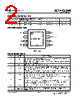
2 / 17 page  ACT4533A/B Rev 0, 14-Aug-13 Innovative Power TM - 2 - www.active-semi.com Copyright © 2013 Active-Semi, Inc. ORDERING INFORMATION PART NUMBER OPERATION AMBIENT TEMPERATURE RANGE OVP/EN PIN PINS PACKING ACT4533BYH-T -40°C to 85°C OVP/EN 8 TAPE & REEL ACT4533AYH-T -40°C to 85°C OVP 8 TAPE & REEL PACKAGE SOP-8EP SOP-8EP PIN CONFIGURATION PIN DESCRIPTIONS PIN NAME DESCRIPTION 1 HSB High Side Bias Pin. This provides power to the internal high-side MOSFET gate driver. Connect a 22nF capacitor from HSB pin to SW pin. 2 IN Power Supply Input. Bypass this pin with a 10µF ceramic capacitor to GND, placed as close to the IC as possible. 3 SW Power Switching Output to External Inductor. 4 GND Ground. Connect this pin to a large PCB copper area for best heat dissipation. Return FB, COMP, and ISET to this GND, and connect this GND to power GND at a single point for best noise immunity. 5 FB Feedback Input. The voltage at this pin is regulated to 0.808V. Connect to the resistor divider between output and GND to set the output voltage. 6 COMP Error Amplifier Output. This pin is used to compensate the converter. 7 EN/OVP ACT4533A:OVP input. If the voltage at this pin exceeds 0.8V, the IC shuts down high- side switch. There is a 4µA pull-up current at this pin. ACT4533B: EN/OVP input. If the voltage at this pin is below 0.65V, the IC remains shut-off; if the Voltage at this pin exceeds 2.26V, the IC shuts down high side switch. There is a 4µA pull-up current at this pin. 8 ISET Output Current Setting Pin. Connect a resistor from ISET to GND to program the output current. Exposed Pad Heat Dissipation Pad. Connect this exposed pad to large ground copper area with copper and vias. |
|
|
リンク URL |
| ALLDATASHEETはお客様のビジネスに役立ちますか? [ DONATE ] |
Alldatasheetは | 広告 | お問い合わせ | プライバシーポリシー | データシートへのリンク | リンク交換 | メーカーリスト All Rights Reserved©Alldatasheet.com |
| Russian : Alldatasheetru.com | Korean : Alldatasheet.co.kr | Spanish : Alldatasheet.es | French : Alldatasheet.fr | Italian : Alldatasheetit.com Portuguese : Alldatasheetpt.com | Polish : Alldatasheet.pl | Vietnamese : Alldatasheet.vn Indian : Alldatasheet.in | Mexican : Alldatasheet.com.mx | British : Alldatasheet.co.uk | New Zealand : Alldatasheet.co.nz |
|
Family Site : ic2ic.com |
icmetro.com |
 Japanese ▼
 English
 Chinese
 German
 Japanese
 Russian
 Korean
 Spanish
 French
 Italian
 Portuguese
 Polish
 Vietnamese
 Indian
 Mexican
 British
 New Zealand