|
データシートサーチシステム |
|
|
データシートサーチシステム |
|
AD1833ACST データシート(PDF) 15 Page - Analog Devices |
|
|
|||||||||||||||||||||||||||||
AD1833ACST データシート(HTML) 15 Page - Analog Devices |
|
|
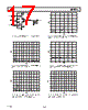
15 / 20 page  REV. 0 AD1833A –15– TDM Mode Timing—Interfacing to a SHARC ® In TDM mode, the AD1833A can be the master or slave, depend- ing on Bit 0 in Control Register 3. In master mode, it generates a frame sync signal (FSTDM) on its L/RCLK pin and a bit clock (BCLKTDM) on its BCLK pin, whereas in slave mode it expects these signals to be provided. These signals are used to control the data transmission from the SHARC. The bit clock must run at a frequency of IMCLK/2 and the interpolation mode must be set to 8 , which limits TDM mode to frequencies of 48 kHz or less. In this mode, all data is written on the rising edge of the bit clock and read on the falling edge of the bit clock. The frame starts with a frame sync at the rising edge of the bit clock. The SHARC then starts outputting data on the next rising edge of the bit clock. Each channel is given a 32-bit clock slot, and the data is left-justified and uses 16, 20, or 24 of the 32 bits. An enlarged diagram detailing this is provided (see Figure 9). The data is sent from the SHARC to the AD1833A on the SDIN1 pin and provided in the following order: MSB first—Internal DACL0, Internal DACL1, Internal DACL2, AUX DACL0, Internal DACR0, Internal DACR1, Internal DACR2, and AUX DACR0. The data is written on the rising edge of the bit clock and read by the AD1833A on the falling edge of the bit clock. The left and right data destined for the auxiliary DAC is sent in standard I 2S format in the next frame using the SDIN2, SDIN3, and SOUT pins as the L/RCLK, BCLK, and SDATA pins, respectively, for communicating with the auxiliary DAC. DSP Mode Timing DSP mode timing uses the rising edge of the frame sync signal on the L/RCLK pin to denote the start of the transmission of a data-word. Note that for both left and right channels, a rising edge is used; therefore in this mode, there is no way to determine which data is intended for the left channel and which is intended for the right. The DSP writes data on the rising edge of BCLK and the AD1833A reads it on the falling edge. The DSP raises the frame sync signal on the rising edge of BCLK and then proceeds to transmit data, MSB first, on the next rising edge of BCLK. The data length can be 16, 20, or 24 bits. The frame sync signal can be brought low any time at or after the MSB is transmitted, but must be brought low at least one BCLK period before the start of the next channel transmission. INTERNAL DAC L0 INTERNAL DAC L1 INTERNAL DAC L2 AUXILIARY DAC L0 INTERNAL DAC R0 INTERNAL DAC R1 INTERNAL DAC R2 AUXILIARY DAC R0 FSTDM BCLKTDM MSB 24-BIT DATA 20-BIT DATA 16-BIT DATA BCLKTDM MSB –1 MSB –2 MSB –3 MSB –4 LSB +8 LSB +7 LSB +6 LSB +5 LSB +4 LSB +3 LSB +2 LSB +1 LSB MSB MSB –1 MSB –2 MSB –3 MSB –4 LSB +4 LSB +3 LSB +2 LSB +1 LSB MSB MSB –1 MSB –2 MSB –3 MSB –4 LSB Figure 9. TDM Mode Timing L/RCLK BCLK SDATA MSB MSB –1 MSB –2 MSB –4 MSB –5 MSB –6 MSB MSB –1 MSB –2 MSB –3 MSB –4 MSB –5 MSB –6 MSB 32 BCLKs 32 BCLKs MSB –3 Figure 10. DSP Mode Timing |
|
|
リンク URL |
| ALLDATASHEETはお客様のビジネスに役立ちますか? [ DONATE ] |
Alldatasheetは | 広告 | お問い合わせ | プライバシーポリシー | データシートへのリンク | リンク交換 | メーカーリスト All Rights Reserved©Alldatasheet.com |
| Russian : Alldatasheetru.com | Korean : Alldatasheet.co.kr | Spanish : Alldatasheet.es | French : Alldatasheet.fr | Italian : Alldatasheetit.com Portuguese : Alldatasheetpt.com | Polish : Alldatasheet.pl | Vietnamese : Alldatasheet.vn Indian : Alldatasheet.in | Mexican : Alldatasheet.com.mx | British : Alldatasheet.co.uk | New Zealand : Alldatasheet.co.nz |
|
Family Site : ic2ic.com |
icmetro.com |
 Japanese ▼
 English
 Chinese
 German
 Japanese
 Russian
 Korean
 Spanish
 French
 Italian
 Portuguese
 Polish
 Vietnamese
 Indian
 Mexican
 British
 New Zealand