|
データシートサーチシステム |
|
|
データシートサーチシステム |
|
HV9961 データシート(PDF) 7 Page - Microchip Technology |
|
|
|||||||||||||||||||||||||||||
HV9961 データシート(HTML) 7 Page - Microchip Technology |
|
|
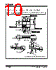
7 / 20 page  2017-2022 Microchip Technology Inc. and its subsidiaries DS20005588B-page 7 HV9961 FIGURE 3-1: Typical Output Characteristic of an HV9961 LED Driver. The short-circuit protection comparator trips when the voltage at CS exceeds 0.44V. When this occurs, the short-circuit gate off-time THICCUP = 400 µs is generated to prevent the staircasing of the inductor current and, potentially, its saturation due to insufficient output voltage. The typical short-circuit inductor current is shown in the waveform of Figure 3-2. FIGURE 3-2: Short-circuit Inductor Current. A leading-edge blanking delay is provided at CS to prevent false triggering of the current feedback and the short-circuit protection. 3.4 Linear Dimming When the voltage at LD falls below 1.5V, the internal 275 mV reference to the constant-current feedback becomes overridden by VLD x 0.185. As long as the current in the inductor remains continuous, the LED current is given by Equation 3-3. However, when VLD falls below 150 mV, the gate output becomes disabled. The gate signal recovers when VLD exceeds 200 mV. It is required in some applications to use the same brightness control signal input to shut off the lamp. The typical linear dimming response is shown in Figure 3-3. FIGURE 3-3: Typical Linear Dimming Response of an HV9961 LED Driver. The linear dimming input could also be used for “mixed-mode” dimming to expand the dimming ratio. In such case, a pulse-width modulated signal with an amplitude below 1.5V should be applied to LD. 3.5 Input Voltage Regulator The HV9961 can be powered directly from an 8 VDC–450 VDC supply through its VIN input. When this voltage is applied at the VIN pin, the HV9961 maintains a constant 7.5V level at VDD. This voltage can be used to power the IC and external circuitry connected to VDD within the rated maximum current or within the thermal ratings of the package, whichever limit is lower. The VDD pin must be bypassed by a low ESR capacitor to provide a low-impedance path for the high-frequency current of the gate output. The HV9961 can also be powered through the VDD pin directly with a voltage greater than the internally regulated 7.5V, but less than 12V. Despite the instantaneous voltage rating of 450V, continuous voltage at VIN is limited by the power dissipation in the package. For example, when HV9961 draws IIN = 2.5 mA from the VIN input, and the 8-pin SOIC package is used, the maximum continuous voltage at VIN is limited to the value shown in Equation 3-5. EQUATION 3-5: V IN = 170VDC HV9961 HV9910B 0 10 2030405060 0.60 0.55 0.50 0.45 0.40 0.35 0.30 0.25 Output Voltage (V) 400µs 0.44V/R CS 0 0.2 0.4 0.6 0.8 1.0 1.2 1.4 1.6 0.40 0.35 0.30 0.25 0.20 0.15 0.10 0.05 0 LD (V) LD Response Characteristics VIN MAX TJMAX TA – R JA IIN -------------------------------- = 396V = Where: Ambient temperature: TA = 25°C Maximum working junction temperature: TJ(MAX) = 125°C Junction-to-ambient thermal resistance: Rθ,JA = 101°C/W |
|
|
リンク URL |
| ALLDATASHEETはお客様のビジネスに役立ちますか? [ DONATE ] |
Alldatasheetは | 広告 | お問い合わせ | プライバシーポリシー | データシートへのリンク | リンク交換 | メーカーリスト All Rights Reserved©Alldatasheet.com |
| Russian : Alldatasheetru.com | Korean : Alldatasheet.co.kr | Spanish : Alldatasheet.es | French : Alldatasheet.fr | Italian : Alldatasheetit.com Portuguese : Alldatasheetpt.com | Polish : Alldatasheet.pl | Vietnamese : Alldatasheet.vn Indian : Alldatasheet.in | Mexican : Alldatasheet.com.mx | British : Alldatasheet.co.uk | New Zealand : Alldatasheet.co.nz |
|
Family Site : ic2ic.com |
icmetro.com |
 Japanese ▼
 English
 Chinese
 German
 Japanese
 Russian
 Korean
 Spanish
 French
 Italian
 Portuguese
 Polish
 Vietnamese
 Indian
 Mexican
 British
 New Zealand