|
データシートサーチシステム |
|
|
データシートサーチシステム |
|
AD4056BCPZ-R2 データシート(PDF) 29 Page - Analog Devices |
|
|
|||||||||||||||||||||||||||||
AD4056BCPZ-R2 データシート(HTML) 29 Page - Analog Devices |
|
|
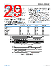
29 / 67 page  Data Sheet AD4050/AD4056 MODES OF OPERATION analog.com Rev. A | 29 of 67 Table 16 shows an overview of the AD4050/AD4056 functional modes. The ADC and serial interface functionality for each mode is given in the subsequent sections. Configuration mode is the default AD4050/AD4056 operating mode following power-up and device resets. The remaining operating modes are selected via the configuration registers as shown in Ta- ble 16. The SPI protocol for register writes and reads is described in the Configuration Mode section. Figure 45 shows the AD4050/AD4056 operating mode selection as a state machine diagram. The ENTER_ADC_MODE bit field controls whether the AD4050/AD4056 is in configuration mode or in one of the five ADC modes as shown in Table 16. Con- figure the ADC_MODE and AUTO_MODE fields before setting ENTER_ADC_MODE to 1'b1 to select the desired operating mode. Setting the ENTER_ADC_MODE to 1'b1 via a register write triggers the AD4050/AD4056 to transition from configuration mode to the selected ADC mode (see Figure 43). The exit command triggers the AD4050/AD4056 to transition from the active ADC mode back to configuration mode. When the AD4050/AD4056 receives the exit command, it internally resets the ENTER_ADC_MODE bit to 1'b0. The exit command consists of the code 5'b10101 clocked in on the SDI pin on the first 5 SCLK rising edges following the CS falling edge. Figure 44 shows a timing diagram for the exit command. The tCONFIG specification indicates the minimum delay between the exit command CS rising edge and when the AD4050/AD4056 can receive new register read and write SPI transactions (see Table 5 and Table 6). Table 16. AD4050/AD4056 Functional Modes Mode ENTER_ADC_MODE ADC_MODE AUTO_MODE POWER_MODE Configuration Mode (Default) 1'b0 Don't Care Don't care 2'b00 Sample Mode 1'b1 2'b00 Don't care 2'b00 Burst Averaging Mode 1'b1 2'b01 Don't care 2'b00 Averaging Mode 1'b1 2'b10 Don't care 2'b00 Monitor Mode 1'b1 2'b11 1'b0 2'b00 Trigger Mode 1'b1 2'b11 1'b1 2'b00 Sleep Mode Don't care Don't care Don't care 2'b11 Figure 43. ENTER_ADC_MODE Timing Diagram Figure 44. Exit Command Timing Diagram |
|
リンク URL |
| ALLDATASHEETはお客様のビジネスに役立ちますか? [ DONATE ] |
Alldatasheetは | 広告 | お問い合わせ | プライバシーポリシー | データシートへのリンク | リンク交換 | メーカーリスト All Rights Reserved©Alldatasheet.com |
| Russian : Alldatasheetru.com | Korean : Alldatasheet.co.kr | Spanish : Alldatasheet.es | French : Alldatasheet.fr | Italian : Alldatasheetit.com Portuguese : Alldatasheetpt.com | Polish : Alldatasheet.pl | Vietnamese : Alldatasheet.vn Indian : Alldatasheet.in | Mexican : Alldatasheet.com.mx | British : Alldatasheet.co.uk | New Zealand : Alldatasheet.co.nz |
|
Family Site : ic2ic.com |
icmetro.com |
 Japanese ▼
 English
 Chinese
 German
 Japanese
 Russian
 Korean
 Spanish
 French
 Italian
 Portuguese
 Polish
 Vietnamese
 Indian
 Mexican
 British
 New Zealand