|
データシートサーチシステム |
|
|
データシートサーチシステム |
|
AD4056BCPZ-R2 データシート(PDF) 12 Page - Analog Devices |
|
|
|||||||||||||||||||||||||||||
AD4056BCPZ-R2 データシート(HTML) 12 Page - Analog Devices |
|
|
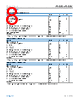
12 / 67 page  Data Sheet AD4050/AD4056 PIN CONFIGURATION AND FUNCTION DESCRIPTIONS analog.com Rev. A | 12 of 67 Table 10. AD4050/AD4056 LFCSP and WLCSP Pin Function Descriptions (Continued) LFCSP Pin No. WLCSP Pin No. Mnemonic Type Description 13 C2 CNV DI Convert Input. In sample mode, averaging mode, and burst averaging mode, a rising edge on the CNV pin initiates a conversion. The CNV pin can optionally be connected to CS. See the Serial Interface section. 14 A2 GP0 DO General Purpose Output 0. The GP0 pin is a digital output that can be configured as multiple device control or interrupt signals. See the Interrupts and Control Signals section. |
|
リンク URL |
| ALLDATASHEETはお客様のビジネスに役立ちますか? [ DONATE ] |
Alldatasheetは | 広告 | お問い合わせ | プライバシーポリシー | データシートへのリンク | リンク交換 | メーカーリスト All Rights Reserved©Alldatasheet.com |
| Russian : Alldatasheetru.com | Korean : Alldatasheet.co.kr | Spanish : Alldatasheet.es | French : Alldatasheet.fr | Italian : Alldatasheetit.com Portuguese : Alldatasheetpt.com | Polish : Alldatasheet.pl | Vietnamese : Alldatasheet.vn Indian : Alldatasheet.in | Mexican : Alldatasheet.com.mx | British : Alldatasheet.co.uk | New Zealand : Alldatasheet.co.nz |
|
Family Site : ic2ic.com |
icmetro.com |
 Japanese ▼
 English
 Chinese
 German
 Japanese
 Russian
 Korean
 Spanish
 French
 Italian
 Portuguese
 Polish
 Vietnamese
 Indian
 Mexican
 British
 New Zealand