|
データシートサーチシステム |
|
|
データシートサーチシステム |
|
ISL91211AII-EV1Z データシート(PDF) 8 Page - Renesas Technology Corp |
|
|
|||||||||||||||||||||||||||||
ISL91211AII-EV1Z データシート(HTML) 8 Page - Renesas Technology Corp |
|
|
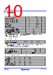
8 / 57 page  FN8922 Rev.3.01 Page 8 of 56 Mar 5, 2020 ISL91211A, ISL91211B 1.5 Pin Descriptions Pin Location Pin Name Type Description A1, B1 PVIN_A Input Power supply for Power Stage A. A2, B2, C2 PH_A Output Switching node for Power Stage A. A3, B3, C3 PGND_A Input Ground connection for Power Stage A. A4, B4, C4 PGND_B Input Ground connection for Power Stage B. A5, B5, C5 PH_B Output Switching node for Power Stage B. A6, B6 PVIN_B Input Power supply for Power Stage B. C1 GPIO0 Input GPIO0. See Table 2 on page 9. This pin is I2C clock for pinmodes 0x0, 0x2, 0x4 through 0x7 and 0xC. C6 WDOG_RST Input Digital input, resets bucks to default output voltage. D1 EN Input Master chip enable input, NMOS logic threshold. D2 GPIO1 Input/Output GPIO1. See Table 2 on page 9. This pin is I2C data for pinmodes 0x0, 0x2, 0x4 through 0x7 and 0xC. D3 INT Output Interrupt line. D4 GPIO2 Input GPIO2. See Table 2 on page 9. D5 GND Input Analog chip ground. D6 RTN1 Input Remote ground sense for Buck1. E1 VOUT4 Input Buck4 output voltage sense for ISL91211B. NOTE: Short to ground for ISL91211A. E2 RTN3 Input Remote ground sense for Buck3. E3 VOUT3 Input Output voltage sense for Buck3. E4 VOUT2 Input Output voltage sense for Buck2. E5 RTN2 Input Remote ground sense for Buck2. E6 VOUT1 Input Remote output voltage sense for Buck1. F1 RTN4 Input Buck4 output voltage sense for ISL91211B. NOTE: Short to ground for ISL91211A. F2 AVIN_FILT Output Filtered analog supply voltage, 2.5V to 5.5V. Place a decoupling capacitor close to the IC. F3 VIO Input I/O supply voltage for digital communications. Nominally connected to 1.8V supply. F4 MPIO0 Input/Output Multipurpose I/O, see Table 2 on page 9. Can be NC if not used. F5 MPIO1 Input/Output Multipurpose I/O, see Table 2 on page 9. Can be NC if not used. Must be pulled up to VIO if using I2C. F6 MPIO2 Input/Output Multipurpose I/O, see Table 2 on page 9. Can be NC if not used. G1 AVIN Input Analog supply voltage, 2.5V to 5.5V. G2, H2, J2 PH_C Output Switching node for Power Stage C. G3, H3, J3 PGND_C Input Ground connection for Power Stage C. G4, H4, J4 PGND_D Input Ground connection for Power Stage D. G5, H5, J5 PH_D Output Switching node for Power Stage D. G6 MPIO3 Input/Output Multipurpose I/O, see Table 2 on page 9. Can be NC if not used. H1, J1 PVIN_C Input Power supply connection for Power Stage C. H6, J6 PVIN_D Input Power supply connection for Power Stage D. |
|
リンク URL |
| ALLDATASHEETはお客様のビジネスに役立ちますか? [ DONATE ] |
Alldatasheetは | 広告 | お問い合わせ | プライバシーポリシー | データシートへのリンク | リンク交換 | メーカーリスト All Rights Reserved©Alldatasheet.com |
| Russian : Alldatasheetru.com | Korean : Alldatasheet.co.kr | Spanish : Alldatasheet.es | French : Alldatasheet.fr | Italian : Alldatasheetit.com Portuguese : Alldatasheetpt.com | Polish : Alldatasheet.pl | Vietnamese : Alldatasheet.vn Indian : Alldatasheet.in | Mexican : Alldatasheet.com.mx | British : Alldatasheet.co.uk | New Zealand : Alldatasheet.co.nz |
|
Family Site : ic2ic.com |
icmetro.com |
 Japanese ▼
 English
 Chinese
 German
 Japanese
 Russian
 Korean
 Spanish
 French
 Italian
 Portuguese
 Polish
 Vietnamese
 Indian
 Mexican
 British
 New Zealand