|
データシートサーチシステム |
|
|
データシートサーチシステム |
|
TSV522IST データシート(PDF) 13 Page - STMicroelectronics |
|
|
|||||||||||||||||||||||||||||
TSV522IST データシート(HTML) 13 Page - STMicroelectronics |
|
|
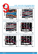
13 / 29 page  5 Application information 5.1 Operating voltages The amplifiers of the TSV52x, TSV52xA series can operate from 2.7 V to 5.5 V. Their parameters are fully specified for 2.7 V, 3.3 V and 5 V power supplies. However, the parameters are very stable in the full VCC range, and several characterization curves show the TSV52x, TSV52xA device characteristics at 2.7 V. Additionally, the main specifications are guaranteed in extended temperature ranges from -40 to +125 °C. 5.2 Common-mode voltage range The TSV52x, TSV52xA devices are built with two complementary PMOS and NMOS input differential pairs. The devices have a rail-to-rail input, and the input common-mode range is extended from VCC- - 0.1 V to VCC+ + 0.1 V. The N channel pair is active for input voltage close to the positive rail typically (VCC+ - 0.7 V) to 100 mv above the positive rail. The P channel pair is active for input voltage close to the negative rail typically 100 mV below the negative rail to VCC- + 0.7 V. And between VCC- + 0.7 V and VCC+ - 0.7 V both N and P pairs are active. When both pairs work together it allows to increase the speed of the TSV52x, TSV52xA devices. This architecture improves the merit factor of the whole device. In the transition region, the performance of CMR, SVR, Vio (Figure 25 and Figure 26) and THD is slightly degraded. Figure 25. Input offset voltage vs. input common-mode at VCC = 2.7 V 0.0 0.0 0.3 0.6 0.6 0.9 1.2 1.2 1.5 1.8 1.8 2.1 2.4 2.4 2.7 -0.8 -0.8 -0.7 -0.6 -0.6 -0.5 -0.4 -0.4 -0.3 -0.2 -0.2 -0.1 0.0 0.0 Vicm (V) AM00481 Figure 26. Input offset voltage vs. input common-mode at VCC = 5.5 V 0.0 0.5 0.9 1.4 1.8 2.3 2.7 3.2 3.6 4.0 4.5 5.0 5.4 -0.8 -0.7 -0.6 -0.5 -0.4 -0.3 -0.2 -0.1 0.0 0.1 Vicm (V) AM00482 5.3 Rail-to-rail input The TSV52x, TSV52xA series are guaranteed without phase reversal as shown in Figure 28. It is extremely important that the current flowing in the input pin does not exceed 10 mA. In order to limit this current, a serial resistor can be added on the Vin path. TSV521, TSV522, TSV524,TSV521A, TSV522A, TSV524A Application information DS8862 - Rev 4 page 13/29 |
|
リンク URL |
| ALLDATASHEETはお客様のビジネスに役立ちますか? [ DONATE ] |
Alldatasheetは | 広告 | お問い合わせ | プライバシーポリシー | データシートへのリンク | リンク交換 | メーカーリスト All Rights Reserved©Alldatasheet.com |
| Russian : Alldatasheetru.com | Korean : Alldatasheet.co.kr | Spanish : Alldatasheet.es | French : Alldatasheet.fr | Italian : Alldatasheetit.com Portuguese : Alldatasheetpt.com | Polish : Alldatasheet.pl | Vietnamese : Alldatasheet.vn Indian : Alldatasheet.in | Mexican : Alldatasheet.com.mx | British : Alldatasheet.co.uk | New Zealand : Alldatasheet.co.nz |
|
Family Site : ic2ic.com |
icmetro.com |
 Japanese ▼
 English
 Chinese
 German
 Japanese
 Russian
 Korean
 Spanish
 French
 Italian
 Portuguese
 Polish
 Vietnamese
 Indian
 Mexican
 British
 New Zealand