|
データシートサーチシステム |
|
|
データシートサーチシステム |
|
TSV522IST データシート(PDF) 14 Page - STMicroelectronics |
|
|
|||||||||||||||||||||||||||||
TSV522IST データシート(HTML) 14 Page - STMicroelectronics |
|
|
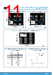
14 / 29 page  Figure 27. Phase reversal test schematic VCC+ VCC- Vout Vinp 5 V 2.5 V AM00483 + _ Figure 28. No phase reversal -2.0 -2.0 -1.0 0.0 0.0 1.0 2.0 2.0 3.0 4.0 4.0 5.0 6.0 6.0 -1 0 1 2 3 4 5 6 VCC = 5.5 V Vinn = 2.75 V Vinp (V) AM00484 5.4 Rail-to-rail output The operational amplifier output levels can go close to the rails: 35 mV maximum above and below the rail when connected to a 10 kΩ resistive load to VCC/2. 5.5 Driving resistive and capacitive loads To drive high capacitive loads, adding an in-series resistor at the output can improve the stability of the device (see Figure 29 for the recommended in series value). Once the in-series resistor has been selected, the stability of the circuit should be tested on the bench and simulated with simulation models. The Rload is placed in parallel with the capacitive load. The Rload and the in-series resistor create a voltage divider which introduces an error proportional to the ratio Rs/Rload. By keeping Rs as low as possible, this error is generally negligible. Figure 29. In-series resistor versus capacitive load 0.1 1.0 10.0 100.0 1 10 100 Stable Minimum serial resistor to be added to a given capacitive load in order to ensure stability VCC = 5 V, Vicm = 2.5 V, T = 25 °C, R load Unstable Capacitive load (nF) AM00485 5.6 Input offset voltage drift over the temperature The maximum input voltage drift over the temperature variation is defined as the offset variation related to offset value measured at 25 °C. The operational amplifier is one of the main circuits of the signal conditioning chain, and the amplifier input offset is a major contributor to the chain accuracy. The signal chain accuracy at 25 °C can be compensated during production at application level. The maximum input voltage drift over temperature enables the system designer to anticipate the effect of temperature variations. The maximum input voltage drift over temperature is computed using Equation 1. TSV521, TSV522, TSV524,TSV521A, TSV522A, TSV524A Application information DS8862 - Rev 4 page 14/29 |
|
リンク URL |
| ALLDATASHEETはお客様のビジネスに役立ちますか? [ DONATE ] |
Alldatasheetは | 広告 | お問い合わせ | プライバシーポリシー | データシートへのリンク | リンク交換 | メーカーリスト All Rights Reserved©Alldatasheet.com |
| Russian : Alldatasheetru.com | Korean : Alldatasheet.co.kr | Spanish : Alldatasheet.es | French : Alldatasheet.fr | Italian : Alldatasheetit.com Portuguese : Alldatasheetpt.com | Polish : Alldatasheet.pl | Vietnamese : Alldatasheet.vn Indian : Alldatasheet.in | Mexican : Alldatasheet.com.mx | British : Alldatasheet.co.uk | New Zealand : Alldatasheet.co.nz |
|
Family Site : ic2ic.com |
icmetro.com |
 Japanese ▼
 English
 Chinese
 German
 Japanese
 Russian
 Korean
 Spanish
 French
 Italian
 Portuguese
 Polish
 Vietnamese
 Indian
 Mexican
 British
 New Zealand