|
データシートサーチシステム |
|
|
データシートサーチシステム |
|
H8SX/1663 データシート(PDF) 561 Page - Renesas Technology Corp |
|
|
|||||||||||||||||||||||||||||
H8SX/1663 データシート(HTML) 561 Page - Renesas Technology Corp |
|
|
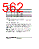
561 / 1158 page  Section 10 16-Bit Timer Pulse Unit (TPU) Rev.1.00 Jun. 07, 2006 Page 509 of 1102 REJ09B0294-0100 10.3.2 Timer Mode Register (TMDR) TMDR sets the operating mode for each channel. The TPU has six TMDR registers, one for each channel. TMDR register settings should be made only while TCNT operation is stopped. 7 1 R 6 1 R 5 BFB 0 R/W 4 BFA 0 R/W 3 MD3 0 R/W 2 MD2 0 R/W 1 MD1 0 R/W 0 MD0 0 R/W Bit Bit Name Initial Value R/W Bit Bit Name Initial Value R/W Description 7, 6 All 1 R Reserved These are read-only bits and cannot be modified. 5 BFB 0 R/W Buffer Operation B Specifies whether TGRB is to normally operate, or TGRB and TGRD are to be used together for buffer operation. When TGRD is used as a buffer register, TGRD input capture/output compare is not generated. In channels 1, 2, 4, and 5, which have no TGRD, bit 5 is reserved. It is always read as 0 and cannot be modified. 0: TGRB operates normally 1: TGRB and TGRD used together for buffer operation 4 BFA 0 R/W Buffer Operation A Specifies whether TGRA is to normally operate, or TGRA and TGRC are to be used together for buffer operation. When TGRC is used as a buffer register, TGRC input capture/output compare is not generated. In channels 1, 2, 4, and 5, which have no TGRC, bit 4 is reserved. It is always read as 0 and cannot be modified. 0: TGRA operates normally 1: TGRA and TGRC used together for buffer operation 3 2 1 0 MD3 MD2 MD1 MD0 0 0 0 0 R/W R/W R/W R/W Modes 3 to 0 Set the timer operating mode. MD3 is a reserved bit. The write value should always be 0. See table 10.12 for details. |
|
リンク URL |
| ALLDATASHEETはお客様のビジネスに役立ちますか? [ DONATE ] |
Alldatasheetは | 広告 | お問い合わせ | プライバシーポリシー | データシートへのリンク | リンク交換 | メーカーリスト All Rights Reserved©Alldatasheet.com |
| Russian : Alldatasheetru.com | Korean : Alldatasheet.co.kr | Spanish : Alldatasheet.es | French : Alldatasheet.fr | Italian : Alldatasheetit.com Portuguese : Alldatasheetpt.com | Polish : Alldatasheet.pl | Vietnamese : Alldatasheet.vn Indian : Alldatasheet.in | Mexican : Alldatasheet.com.mx | British : Alldatasheet.co.uk | New Zealand : Alldatasheet.co.nz |
|
Family Site : ic2ic.com |
icmetro.com |
 Japanese ▼
 English
 Chinese
 German
 Japanese
 Russian
 Korean
 Spanish
 French
 Italian
 Portuguese
 Polish
 Vietnamese
 Indian
 Mexican
 British
 New Zealand