Preliminary
8-128
RF2488
Rev A0 010905
8
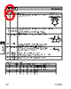
RF2488 State Control Truth Table
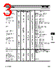
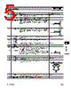
Pin
Function
Description
Interface Schematic
16
IF1-
IF output. Open collector output, requires external matching compo-
nents and DC connection to VCC.
17
IF1+
IF output. Open collector output, requires external matching compo-
nents and DC connection to VCC.
See pin 16.
18
BAND SEL
This CMOS compatible pin controls the selection of the low or high
band signal path (See the State Control Truth Table). Local bypass
capacitor required.
19
Low LO IN
LO band local oscillator input. This pin is AC-coupled and matched to
50
Ω.
20
TX/RX
This CMOS compatible TX/RX mode select Power Control Pin. CMOS
compatible signal controlling the functional state of the device (See the
State Control Truth Table). Local bypass capacitor required.
21
Low MIX IN
Low band RF mixer input. Although the base of the mixer input transis-
tor is AC coupled, this pin serves a dual purpose of providing a DC bias
path via external inductor to GND. The typical input impedance is 8
Ω
real and requires external matching to 50
Ω.
22
VCC BIAS
Bias supply voltage. Local bypass capacitor required.
23
Low LNA
OUT
Low band LNA output. Bias for the LNA is provided through this pin,
hence it should be connected to VCC through and inductor.
See pin 3.
24
Low LNA
VCC
Low band LNA RF supply voltage. Local bypass capacitor required.
State
TX/RX
Band Sel
IF Out Sel
Active Circuits
0000
Low Band LNA, IF1 Mixer
1001
Low Band LNA, IF2 Mixer
2010
High Band LNA, IF1 Mixer
3011
High Band LNA, IF2 Mixer
4100
All Off
5101
All Off
6110
All Off
7111
All Off
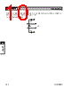
IF1+
IF1-
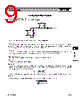
1pF
1pF
1pF
LO IN
500
Ω
Low MIX IN


 Japanese ▼
 English
 Chinese
 German
 Japanese
 Russian
 Korean
 Spanish
 French
 Italian
 Portuguese
 Polish
 Vietnamese
 Indian
 Mexican
 British
 New Zealand