|
データシートサーチシステム |
|
|
データシートサーチシステム |
|
AS3687 データシート(PDF) 10 Page - ams AG |
|
|
|||||||||||||||||||||||||||||
AS3687 データシート(HTML) 10 Page - ams AG |
|
|
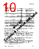
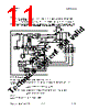
10 / 55 page  AS3687/87XM Datasheet www.austriamicrosystems.com/AS3687 1v3-4 9 - 54 Table 3 – Step Up DC/DC Converter Parameters Symbol Parameter Min TYP Max Unit Note Vrsense_max 46 66 85 e.g., 0.66A for 0.1 Ω sense resistor Vrsense_max_st art 25 33 43 For fixed startup time of 500us Vrsense_max_lc Current Limit Voltage at RSENSE (R1) 30 43 57 mV If stepup_lowcur= 1 RSW Switch Resistance 1 Ω ON-resistance of external switching transistor. 0 55 At 16V output voltage. Iload Load Current 0 35 mA At 25V output voltage. fIN Switching Frequency 0.9 1 1.1 MHz Internally trimmed. Cout Output Capacitor 0.7 4.7 µ F Ceramic, ±20%. Use nominal 4.7 μF capacitors to obtain at least 0.7µF under all conditions (voltage dependance of capacitors) L Inductor 7 10 13 µ H Use inductors with small Cparasitic (<100pF) to get high efficiency. tMIN_ON Minimum on Time 90 140 190 ns MDC Maximum Duty Cycle 88 91 % Voltage ripple >20kHz 160 mV Vripple Voltage ripple <20kHz 40 mV Cout=4.7uF,Iout=0..45mA, Vbat=3.0...4.2V Efficiency Efficiency 85 % Iout=20mA,Vout=17V,Vbat=3.8V To ensure soft startup of the dcdc converter, the overcurrent limits are reduced for a fixed time after enabling the dcdc converter. The total startup time for an output voltage of e.g. 25V is less than 2ms. 7.1.1 Feedback Selection Register 12 (DCDC Control) selects the type of feedback for the Step Up DC/DC Converter. The feedback for the DC/DC converter can be selected either by current sinks (CURR1, CURR2, CURR6) or by a voltage feedback at pin DCDC_FB. If the register bit step_up_fb_auto is set, the feedback path is automatically selected between CURR1, CURR2 and CURR6 (the lowest voltage of these current sinks is used). Setting step_up_fb enables feedback on the pins CURR1, CURR2 or CURR6. The Step Up DC/DC Converter is regulated such that the required current at the feedback path can be supported. (Bit step_up_res should be set to 0 in this configuration) Note : Always choose the path with the highest voltage drop as feedback to guarantee adequate supply for the other (unregulated) paths or enable the register bit step_up_fb_auto. 7.1.2 Overvoltage Protection in Current Feedback Mode The overvoltage protection in current feedback mode (step_up_fb = 01, 10 or 11 or step_up_fb_auto = 1) works as follows: Only resistor R3 and C10/C11 is soldered and R4 is omitted. An internal current source (sink) is used to generate a voltage drop across the resistor R3. If then the voltage on DCDC_FB is above 1.25V, the DCDC is momentarily disabled to avoid too high voltages on the output of the DCDC converter. The protection voltage can be calculated according to the following formula: VPROTECT = 1.25V + IDCDC_FB * R2 |
|
リンク URL |
| ALLDATASHEETはお客様のビジネスに役立ちますか? [ DONATE ] |
Alldatasheetは | 広告 | お問い合わせ | プライバシーポリシー | データシートへのリンク | リンク交換 | メーカーリスト All Rights Reserved©Alldatasheet.com |
| Russian : Alldatasheetru.com | Korean : Alldatasheet.co.kr | Spanish : Alldatasheet.es | French : Alldatasheet.fr | Italian : Alldatasheetit.com Portuguese : Alldatasheetpt.com | Polish : Alldatasheet.pl | Vietnamese : Alldatasheet.vn Indian : Alldatasheet.in | Mexican : Alldatasheet.com.mx | British : Alldatasheet.co.uk | New Zealand : Alldatasheet.co.nz |
|
Family Site : ic2ic.com |
icmetro.com |
 Japanese ▼
 English
 Chinese
 German
 Japanese
 Russian
 Korean
 Spanish
 French
 Italian
 Portuguese
 Polish
 Vietnamese
 Indian
 Mexican
 British
 New Zealand