|
データシートサーチシステム |
|
|
データシートサーチシステム |
|
LTC1258 データシート(PDF) 5 Page - Linear Technology |
|
|
|||||||||||||||||||||||||||||
LTC1258 データシート(HTML) 5 Page - Linear Technology |
|
|
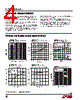
5 / 8 page  LTC1258 Series 5 1258sfb TYPICAL PERFORMANCE CHARACTERISTICS LTC1258-2.5 Output Voltage vs Input Voltage LTC1258-2.5 Input Current vs Input Voltage LTC1258-2.5 PSRR vs Frequency LTC1258-2.5 0.1Hz to 10Hz Noise LTC1258-5 Input Current vs Input Voltage in Dropout LTC1258-2.5 Input Current vs Input Voltage in Dropout INPUT VOLTAGE (V) 2 2.5010 2.5005 2.5000 2.4995 4 68 10 1258 G07 12 14 TA = 25°C INPUT VOLTAGE (V) 2 7 6 5 4 4 68 10 1258 G08 12 14 TA = 25°C FREQUENCY (Hz) 60 50 40 30 20 10 0 10 1k 10k 1258 G09 100 VIN = 2.7V 5μV/DIV 1258 G10 1SEC/DIV VIN = 2.7V INPUT VOLTAGE (V) 0123456789 10 1258 G11 1400 1200 1000 800 600 400 200 0 TA = –55°C TA = 25°C TA = 125°C INPUT VOLTAGE (V) 0 0.5 1 1.5 2 2.5 3 3.5 4 4.5 5 1258 G12 250 200 150 100 50 0 TA = 25°C TA = –55°C TA = 125°C PIN FUNCTIONS OUT (Pin 1): Reference Output. The output can source up to 10mA and sink up to 2mA. It is stable with output bypass capacitor ranging from 0μF to 1μF. IN (Pin 2): Positive Supply. Bypassing with a 0.1μF ca- pacitor is recommended if the output loading changes. (VOUT + 0.2V) ≤ VIN ≤ 12.6V. DNC (Pin 3): (LTC1258-2.5/LTC1258-3/LTC1258-4.1/ LTC1258-5) Do Not Connect. Connected internally for post package trim. This pin must be left unconnected. FB (Pin 3): (LT1258) Resistor Divider Feedback Pin. Con- nect a resistor divider from OUT to GND and the center tap to FB. This pin sets the output potential. VV RR R OUT = + ⎛ ⎝⎜ ⎞ ⎠⎟ 2 385 12 2 .;R1 is connected from OUT to FB and R2 from FB to GND. GND (Pin 4): Negative Supply or Ground Connection. DNC (Pins 5, 6, 7, 8): Do Not Connect. Connected in- ternally for post package trim. These pins must be left unconnected. |
|
|
リンク URL |
| ALLDATASHEETはお客様のビジネスに役立ちますか? [ DONATE ] |
Alldatasheetは | 広告 | お問い合わせ | プライバシーポリシー | データシートへのリンク | リンク交換 | メーカーリスト All Rights Reserved©Alldatasheet.com |
| Russian : Alldatasheetru.com | Korean : Alldatasheet.co.kr | Spanish : Alldatasheet.es | French : Alldatasheet.fr | Italian : Alldatasheetit.com Portuguese : Alldatasheetpt.com | Polish : Alldatasheet.pl | Vietnamese : Alldatasheet.vn Indian : Alldatasheet.in | Mexican : Alldatasheet.com.mx | British : Alldatasheet.co.uk | New Zealand : Alldatasheet.co.nz |
|
Family Site : ic2ic.com |
icmetro.com |
 Japanese ▼
 English
 Chinese
 German
 Japanese
 Russian
 Korean
 Spanish
 French
 Italian
 Portuguese
 Polish
 Vietnamese
 Indian
 Mexican
 British
 New Zealand