|
データシートサーチシステム |
|
|
データシートサーチシステム |
|
TPS65023 データシート(PDF) 10 Page - Texas Instruments |
|
|
|||||||||||||||||||||||||||||
TPS65023 データシート(HTML) 10 Page - Texas Instruments |
|
|
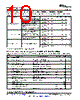
10 / 47 page  TPS65023, TPS65023B SLVS670K – JUNE 2006 – REVISED DECEMBER 2015 www.ti.com 7.6 Electrical Characteristics: Supply Pins VCC, VINDCDC1, VINDCDC2, VINDCDC3 VINDCDC1 = VINDCDC2 = VINDCDC3 = VCC = VINLDO = 3.6 V, VBACKUP = 3 V, TA = –40°C to 85°C (unless otherwise noted) PARAMETER TEST CONDITIONS MIN TYP(1) MAX UNIT All 3 DCDC converters enabled, zero VCC = 3.6 V, VBACKUP = 3 V; 85 100 load, and no switching, LDOs enabled V(VSYSIN) = 0 V All 3 DCDC converters enabled, zero VCC = 3.6 V, VBACKUP = 3 V; 78 90 load, and no switching, LDOs off V(VSYSIN) = 0 V Operating quiescent I(q) μA DCDC1 and DCDC2 converters current, PFM VCC = 3.6 V, VBACKUP = 3 V; enabled, zero load, and no switching, 57 70 V(VSYSIN) = 0 V LDOs off DCDC1 converter enabled, zero load, VCC = 3.6 V, VBACKUP = 3 V; 43 55 and no switching, LDOs off V(VSYSIN) = 0 V All 3 DCDC converters enabled and VCC = 3.6 V, VBACKUP = 3 V; 2 3 running in PWM, LDOs off V(VSYSIN) = 0 V DCDC1 and DCDC2 converters VCC = 3.6 V, VBACKUP = 3 V; II Current into VCC; PWM enabled and running in PWM, LDOs 1.5 2.5 mA V(VSYSIN) = 0 V off DCDC1 converter enabled and running VCC = 3.6 V, VBACKUP = 3 V; 0.85 2 in PWM, LDOs off V(VSYSIN) = 0 V VCC = 3.6 V, VBACKUP = 3 V; 23 33 μA V(VSYSIN) = 0 V VCC = 2.6 V, VBACKUP = 3 V; I(q) Quiescent current All converters disabled, LDOs off 3.5 5 μA V(VSYSIN) = 0 V VCC = 3.6 V, VBACKUP = 0 V; 43 μA V(VSYSIN) = 0 V (1) Typical values are at TA = 25°C, unless otherwise noted. 7.7 Electrical Characteristics: Supply Pins VBACKUP, VSYSIN, VRTC, VINLDO VINDCDC1 = VINDCDC2 = VINDCDC3 = VCC = VINLDO = 3.6 V, VBACKUP = 3 V, TA = –40°C to 85°C (unless otherwise noted) PARAMETER TEST CONDITIONS MIN TYP(1) MAX UNIT VBACKUP, VSYSIN, VRTC VBACKUP = 3 V, VSYSIN = 0 V; I(q) Operating quiescent current 20 33 μA VCC = 2.6 V, current into VBACKUP VBACKUP < V_VBACKUP, current into I(SD) Operating quiescent current 2 3 μA VBACKUP VRTC LDO output voltage VSYSIN = VBACKUP = 0 V, IO = 0 mA 3 V IO Output current for VRTC VSYSIN < 2.57 V and VBACKUP < 2.57 V 30 mA VRTC short-circuit current limit VRTC = GND; VSYSIN = VBACKUP = 0 V 100 mA Maximum output current at VRTC for VRTC > 2.6 V, VCC = 3 V; 30 mA RESPWRON = 1 VSYSIN = VBACKUP = 0 V VO Output voltage accuracy for VRTC VSYSIN = VBACKUP = 0 V; IO = 0 mA –1% 1% Line regulation for VRTC VCC = VRTC + 0.5 V to 6.5 V, IO = 5 mA –1% 1% IO = 1 mA to 30 mA; Load regulation VRTC –3% 1% VSYSIN = VBACKUP = 0 V Regulation time for VRTC Load change from 10% to 90% 10 μs Ilkg Input leakage current at VSYSIN VSYSIN < V_VSYSIN 2 μA rDS(on) of VSYSIN switch 12.5 Ω rDS(on) of VBACKUP switch 12.5 Ω Input voltage range at VBACKUP(2) 2.73 3.75 V Input voltage range at VSYSIN(2) 2.73 3.75 V VSYSIN threshold VSYSIN falling –3% 2.55 3% V (1) Typical values are at TA = 25°C, unless otherwise noted. (2) Based on the requirements for the Intel PXA270 processor. 10 Submit Documentation Feedback Copyright © 2006–2015, Texas Instruments Incorporated Product Folder Links: TPS65023 TPS65023B |
|
リンク URL |
| ALLDATASHEETはお客様のビジネスに役立ちますか? [ DONATE ] |
Alldatasheetは | 広告 | お問い合わせ | プライバシーポリシー | データシートへのリンク | リンク交換 | メーカーリスト All Rights Reserved©Alldatasheet.com |
| Russian : Alldatasheetru.com | Korean : Alldatasheet.co.kr | Spanish : Alldatasheet.es | French : Alldatasheet.fr | Italian : Alldatasheetit.com Portuguese : Alldatasheetpt.com | Polish : Alldatasheet.pl | Vietnamese : Alldatasheet.vn Indian : Alldatasheet.in | Mexican : Alldatasheet.com.mx | British : Alldatasheet.co.uk | New Zealand : Alldatasheet.co.nz |
|
Family Site : ic2ic.com |
icmetro.com |
 Japanese ▼
 English
 Chinese
 German
 Japanese
 Russian
 Korean
 Spanish
 French
 Italian
 Portuguese
 Polish
 Vietnamese
 Indian
 Mexican
 British
 New Zealand