|
データシートサーチシステム |
|
|
データシートサーチシステム |
|
LM10506 データシート(PDF) 20 Page - Texas Instruments |
|
|
|||||||||||||||||||||||||||||
LM10506 データシート(HTML) 20 Page - Texas Instruments |
|
|
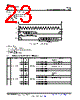
20 / 43 page  LM10506 SNVS729F – SEPTEMBER 2011 – REVISED AUGUST 2014 www.ti.com Device Functional Modes (continued) 8.3.4.1 STANDBY Pin When the STANDBY pin is asserted high, the LM10506 will enter Standby Mode. While in Standby Mode, Buck 1 and Buck 2 are disabled. Buck 3’s output voltage is transitioned to the PSML (Programmable Standby Mode Level) as set by register 0x09. The STANDBY pin is internally pulled down, and there is a 1 second delay during powerup before the state of the STANDBY pin is checked. NOTE If Buck 1 and Buck 2 are already disabled, and the STANDBY pin is asserted high, then Buck 3 will not go to PSML – for further instructions, see STANDBY Programming via SPI. Bucks 1 and 2 will be ramped down when the disable signal is given. Buck 1 starts ramping 2 ms after Buck 2 has started ramping. Entering Standby Sequence will be: 1. Buck 3 → PSML (Programmable Standby Mode Level) 2. 2 ms delay 3. Buck 2 → Disabled 4. 2 ms delay 5. Buck 1 → Disabled An internal pulldown resistor 22 k Ω (±30%) is attached to the FB pin of Buck 1 and Buck 2. The outputs of Buck 1 and 2 are pulled to ground level when they are disabled to discharge any residual charge present in the output circuitry. When STANDBY transitions to a low, Buck 1 is again enabled followed by Buck 2. Buck 3 will go back to its previous state. When waking up from Standby, the sequence will be: 1. Buck 1 → Previous State 2. 2 ms delay 3. Buck 2 and Buck 3 transition together → Previous State 8.3.4.2 Standby Programming Via SPI There is no bit which has the same function as the STANDBY pin. There is only one requirement programming LM10506 into Standby Mode via SPI. Setting LDO Sleep Mode bit high must be the last move when entering Standby Mode and programming the bit low when waking from Standby Mode must be the first move. Disabling or programming the Bucks to new level is the user’s decision based on power consumption and other requirements. The following section describes how to program the chip into Standby Mode corresponding to STANDBY PIN function. To program the LM10506 to Standby Mode via SPI Buck 1 and Buck 2 must be disabled by host device (Register 0x0A bit 1 and 0). Buck 3 must be programmed to desired level using Register 0x00. After Buck 3 has finished ramping LDO Sleep Mode bit must be set high (Register 0x0E bit 1). To wake LM10506 from Standby Mode LDO Sleep Mode bit must be set low (Register 0x0E bit 1). Bucks 1 and 2 must be enabled. Buck 3 voltage must be programmed to previous output level. For LM10506 -C, -D,when Buck 1 is re-enabled upon exiting STANDBY, soft start will engage. 8.3.4.3 Standby Mode, Operational Constraints In Standby mode the device is in a low power mode. All internal clocks are turned off to conserve power and Buck 3 will only operate in PFM mode. While limited to PFM mode the loading on Buck 3 should be kept below 80 mA typ. to remain below the PFM/PWM threshold and avoid device shutdown. It is recommended that the device loading should be lowered accordingly prior to entering standby mode via STANDBY. 20 Submit Documentation Feedback Copyright © 2011–2014, Texas Instruments Incorporated Product Folder Links: LM10506 |
|
リンク URL |
| ALLDATASHEETはお客様のビジネスに役立ちますか? [ DONATE ] |
Alldatasheetは | 広告 | お問い合わせ | プライバシーポリシー | データシートへのリンク | リンク交換 | メーカーリスト All Rights Reserved©Alldatasheet.com |
| Russian : Alldatasheetru.com | Korean : Alldatasheet.co.kr | Spanish : Alldatasheet.es | French : Alldatasheet.fr | Italian : Alldatasheetit.com Portuguese : Alldatasheetpt.com | Polish : Alldatasheet.pl | Vietnamese : Alldatasheet.vn Indian : Alldatasheet.in | Mexican : Alldatasheet.com.mx | British : Alldatasheet.co.uk | New Zealand : Alldatasheet.co.nz |
|
Family Site : ic2ic.com |
icmetro.com |
 Japanese ▼
 English
 Chinese
 German
 Japanese
 Russian
 Korean
 Spanish
 French
 Italian
 Portuguese
 Polish
 Vietnamese
 Indian
 Mexican
 British
 New Zealand