|
データシートサーチシステム |
|
|
データシートサーチシステム |
|
NM29N16 データシート(PDF) 3 Page - National Semiconductor (TI) |
|
|
|
|||||||||||||||||||||||||||||
NM29N16 データシート(HTML) 3 Page - National Semiconductor (TI) |
|
|
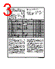
3 / 30 page  Absolute Maximum Ratings If MilitaryAerospace specified devices are required please contact the National Semiconductor Sales OfficeDistributors for availability and specifications Power Supply (VCC) b 06V to 70V Input Voltage (VIN) b 06V to 70V InputOutput Voltage (VIO) b 06V to VCC g05V (s7V) Power Dissipation (PD) 05W Soldering Temperature (Tsolder) (10 seconds) 260 C Storage Temperature (Tstg) b 55 Cto150 C Operating Temperature (Topr)0 Cto70 C Recommended Operating Conditions Min Typ Max Units Power Supply (VCC) 45 50 55 V High Level Input Voltage (VIH) 24 VCC a 05 V Low Level Input Voltage (VIL) b03 08 V b 2V (Pulse Width k 20 ns) DC Operating Characteristics (TA e 0 Cto70 C VCC e 5V g10%) Symbol Parameter Conditions Min Typ Max Units ILI Input Leakage Current VIN e 0V to VCC g 10 m A ILO Output Leakage Current VOUT e 04V to VCC g 10 m A ICC01 Operating Current (Serial Read) CE e VIL tCYCLE e 80 ns 15 30 mA ICC02 Operating Current (Serial Read) IOUT e 0mA tCYCLE e 1 ms5 mA ICC03 Operating Current (Command Input) tCYCLE e 80 ns 15 30 mA ICC04 Operating Current (Data Input) tCYCLE e 80 ns 50 70 mA ICC05 Operating Current (Address Input) tCYCLE e 80 ns 15 30 mA ICC06 Operating Current (Register Read) tCYCLE e 80 ns 15 30 mA ICC07 Programming Current 40 60 mA ICC08 Erasing Current 20 40 mA ICCS1 Standby Current CE e VIH 1mA ICCS2 Standby Current CE e VCC b 02V 100 m A VOH High Level Output Voltage IOH eb400 mA 24 V VOL Low Level Output Voltage IOL e 21 mA 04 V IOL(RB) Output Current of (RB) Pin VOL e 04V 10 mA Pin Functions The NM29N16 is a sequential access memory which utilizes time sharing input of address and data information Command Latch Enable CLE The CLE input signal is used to control the input of commands into the internal command register The command is latched into the com- mand register from the IO port at the rising edge of the WE signal while CLE is high Address Latch Enable ALE The ALE signal is used to control the input of either address information or input data into the internal addressdata register Address information is latched at the rising edge of WE if ALE is high Input data is latched if ALE is low Chip Enable CE The device goes into a low power stand- by mode during a read operation when CE goes high The CE signal is ignored when the device is in a busy state (RB e L) such as during a program or erase operation and will not go into standby mode if a CE high signal is input Write Enable WE The WE signal is used to strobe data into the IO port Read Enable RE The RE signal strobes data output Data is available tREA after the falling edge of RE The internal column address counter is also incremented (Address a 1) with this falling edge IO Port IO 1 – 8 The IO 1 – 8 pins are used as the port for transferring address command and inputoutput data infor- mation to or from the device Write Protect WP The WP signal is used to protect the device from inadvertent programming or erasing The inter- nal voltage regulator is reset when WP is low This signal is usually used for protecting the data during the power onoff sequence when the input signals are invalid ReadyBusy RB The RB output signal is used to indi- cate the operating condition of the device The RB signal is in a busy state (RB e L) during the program erase or read operations and will return to a ready state (RB e H) after completion The output buffer of this signal is an open drain http www nationalcom 3 |
|
リンク URL |
| ALLDATASHEETはお客様のビジネスに役立ちますか? [ DONATE ] |
Alldatasheetは | 広告 | お問い合わせ | プライバシーポリシー | データシートへのリンク | リンク交換 | メーカーリスト All Rights Reserved©Alldatasheet.com |
| Russian : Alldatasheetru.com | Korean : Alldatasheet.co.kr | Spanish : Alldatasheet.es | French : Alldatasheet.fr | Italian : Alldatasheetit.com Portuguese : Alldatasheetpt.com | Polish : Alldatasheet.pl | Vietnamese : Alldatasheet.vn Indian : Alldatasheet.in | Mexican : Alldatasheet.com.mx | British : Alldatasheet.co.uk | New Zealand : Alldatasheet.co.nz |
|
Family Site : ic2ic.com |
icmetro.com |
 Japanese ▼
 English
 Chinese
 German
 Japanese
 Russian
 Korean
 Spanish
 French
 Italian
 Portuguese
 Polish
 Vietnamese
 Indian
 Mexican
 British
 New Zealand