 |
データシートサーチシステム |
|
|
データシートサーチシステム |
|
The question interval is too short.
Please try again in a few seconds.

Hello, Please ask a question about AK8180D Datasheet
# Example questions:
➢ What are the conditions under which the propagation delay needs to be considered from the 3v table versus the 5v table?
➢ What package type is the ak8180d available in, and what are some key dimensions provided in the datasheet?
➢ What are the functional differences between using dsela/b/c set to '0' versus '1'?
| Part No. | AK8180D |
| Manufacturer | AKM |
| Size | 832 Kbytes |
| Pages | 12 pages |
| Description | 2.5V, 3.3V LVCMOS 1:10 Clock Fanout Buffer |

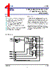






1. Overview & Purpose:
️· The AK8180D is a high-performance, mixed-signal clock distribution device from Asahi Kasei Microdevices (AKM). It's designed to distribute clock signals with precision.
️· It caters to applications that need multiple clocks with flexibility and low jitter.
2. Key Features:
️· Multiple Clock Outputs: The device offers a number of clock outputs (QA0-2, QB0-2, QC0-3), allowing for flexibility in distribution.
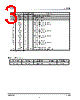
️· Clock Division: Outputs can be configured to run at either half or full speed of a reference clock (REFCLK), controlled by DSELA, DSELB, and DSELC pins.
️· Output Enable (OE) / Reset (MR): OE pin enables or disables outputs. The MR pin performs an internal reset, putting outputs in a high-impedance state.
️· Low Jitter: Designed for minimal jitter in the distributed clock signals.
️· Mixed Supply Voltage Support: The datasheet indicates operation with a combination of 3.3V and 2.5V supply voltages.
️· RoHS Compliant: Meets environmental regulations for lead-free components.
3. Specifications (Key Points - Refer to the Datasheet for Complete Details):
️· Supply Voltage: 3.3V and 2.5V support.
️· Input Clock (REFCLK): Frequency range needs to be confirmed with the datasheet tables.
️· Output Frequency: Dependent on REFCLK and the configuration of the DSEL pins.
️· Jitter: Low jitter performance - specific values will be in the AC characteristics tables.
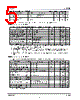
️· Output Pulse Skew (tskO): 200-250 ps (Typical, based on tables).
️· Device-to-Device Skew (tskD): < 3 ns.
️· Output Duty Cycle: 45-55% (Typical).
️· Operating Temperature: -40°C to +85°C
4. Functional Operation/Control Pins:
️· DSELA, DSELB, DSELC: Select whether the respective output groups (QA, QB, QC) operate at half or full REFCLK speed.
️· OE: Output Enable. Active Low.
️· MR: Master Reset. Places outputs in high-impedance state.
5. Package Information:
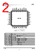
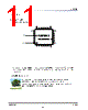
️· 32-lead LQFP (Low Profile Quad Flat Package)
️· Specific dimensions are provided in the datasheet figures.
6. Important Notices/Legal Disclaimers:
️· Product Changes: AKM reserves the right to change specifications without notice.
️· Liability Disclaimer: AKM disclaims liability for any losses or damages resulting from the use of these products.
️· Restricted Use: AKM products are not intended for use in safety-critical or life-support systems without explicit written consent.
️· Export Control: Export restrictions may apply.
Where to Find More Specifics:
️· AC Characteristics Tables: These tables are critical for understanding the timing performance (jitter, skew, duty cycle). Refer to the datasheet's AC Characteristics sections for values.
️· Functional Diagrams & Timing Diagrams: These visual aids help illustrate the device's operation and provide clear timing relationships.
️· Figure 1-5: These diagrams help explain the device’s input reference, output translation time, propagation delay, output skew, and output duty cycle.
1. Overview & Purpose:
️· The AK8180D is a high-performance, mixed-signal clock distribution device from Asahi Kasei Microdevices (AKM). It's designed to distribute clock signals with precision.
️· It caters to applications that need multiple clocks with flexibility and low jitter.
2. Key Features:
️· Multiple Clock Outputs: The device offers a number of clock outputs (QA0-2, QB0-2, QC0-3), allowing for flexibility in distribution.
️· Clock Division: Outputs can be configured to run at either half or full speed of a reference clock (REFCLK), controlled by DSELA, DSELB, and DSELC pins.
️· Output Enable (OE) / Reset (MR): OE pin enables or disables outputs. The MR pin performs an internal reset, putting outputs in a high-impedance state.
️· Low Jitter: Designed for minimal jitter in the distributed clock signals.
️· Mixed Supply Voltage Support: The datasheet indicates operation with a combination of 3.3V and 2.5V supply voltages.
️· RoHS Compliant: Meets environmental regulations for lead-free components.
3. Specifications (Key Points - Refer to the Datasheet for Complete Details):
️· Supply Voltage: 3.3V and 2.5V support.
️· Input Clock (REFCLK): Frequency range needs to be confirmed with the datasheet tables.
️· Output Frequency: Dependent on REFCLK and the configuration of the DSEL pins.
️· Jitter: Low jitter performance - specific values will be in the AC characteristics tables.
️· Output Pulse Skew (tskO): 200-250 ps (Typical, based on tables).
️· Device-to-Device Skew (tskD): < 3 ns.
️· Output Duty Cycle: 45-55% (Typical).
️· Operating Temperature: -40°C to +85°C
4. Functional Operation/Control Pins:
️· DSELA, DSELB, DSELC: Select whether the respective output groups (QA, QB, QC) operate at half or full REFCLK speed.
️· OE: Output Enable. Active Low.
️· MR: Master Reset. Places outputs in high-impedance state.
5. Package Information:
️· 32-lead LQFP (Low Profile Quad Flat Package)
️· Specific dimensions are provided in the datasheet figures.
6. Important Notices/Legal Disclaimers:
️· Product Changes: AKM reserves the right to change specifications without notice.
️· Liability Disclaimer: AKM disclaims liability for any losses or damages resulting from the use of these products.
️· Restricted Use: AKM products are not intended for use in safety-critical or life-support systems without explicit written consent.
️· Export Control: Export restrictions may apply.
Where to Find More Specifics:
️· AC Characteristics Tables: These tables are critical for understanding the timing performance (jitter, skew, duty cycle). Refer to the datasheet's AC Characteristics sections for values.
️· Functional Diagrams & Timing Diagrams: These visual aids help illustrate the device's operation and provide clear timing relationships.
️· Figure 1-5: These diagrams help explain the device’s input reference, output translation time, propagation delay, output skew, and output duty cycle.
| Part No. | AK8180D |
| Manufacturer | AKM |
| Size | 832 Kbytes |
| Pages | 12 pages |
| Description | 2.5V, 3.3V LVCMOS 1:10 Clock Fanout Buffer |
| ALLDATASHEETはお客様のビジネスに役立ちますか? [ DONATE ] |
Alldatasheetは | 広告 | お問い合わせ | プライバシーポリシー | データシートへのリンク | リンク交換 | メーカーリスト All Rights Reserved©Alldatasheet.com |
| Russian : Alldatasheetru.com | Korean : Alldatasheet.co.kr | Spanish : Alldatasheet.es | French : Alldatasheet.fr | Italian : Alldatasheetit.com Portuguese : Alldatasheetpt.com | Polish : Alldatasheet.pl | Vietnamese : Alldatasheet.vn Indian : Alldatasheet.in | Mexican : Alldatasheet.com.mx | British : Alldatasheet.co.uk | New Zealand : Alldatasheet.co.nz |
|
Family Site : ic2ic.com |
icmetro.com |
 Japanese ▼
  English
 Chinese
 German
 Russian
 Korean
 Spanish
 French
 Italian
 Portuguese
 Polish
 Vietnamese
 Indian
 Mexican
 British
 New Zealand