|
データシートサーチシステム |
|
|
データシートサーチシステム |
|
AK8180D データシート(PDF) 4 Page - Asahi Kasei Microsystems |
|
|
|||||||||||||||||||||||||||||
AK8180D データシート(HTML) 4 Page - Asahi Kasei Microsystems |
|
|
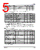
4 / 12 page  AK8180D Oct-2011 MS1306-E-01 - 4 - Absolute Maximum Rating Over operating free-air temperature range unless otherwise noted (1) Items Symbol Ratings Unit Supply voltage VDD -0.3 to 4.6 V Input voltage Vin GND-0.3 to VDD+0.3 V Input current (any pins except supplies) IIN ±10 mA Storage temperature Tstg -55 to 130 C Note (1) Stress beyond those listed under “Absolute Maximum Ratings” may cause permanent damage to the device. These are stress ratings only. Functional operation of the device at these or any other conditions beyond those indicated under “Recommended Operating Conditions” is not implied. Exposure to absolute-maximum-rating conditions for extended periods may affect device reliability. Electrical parameters are guaranteed only over the recommended operating temperature range. This device is manufactured on a CMOS process, therefore, generically susceptible to damage by excessive static voltage. Failure to observe proper handling and installation procedures can cause damage. AKM recommends that this device is handled with appropriate precautions. Recommended Operation Conditions Parameter Symbol Conditions Min Typ Max Unit Operating temperature Ta -40 85 C Supply voltage (1) VDD VDD 5% 2.375 2.5 2.625 V 3.135 3.3 3.465 (1) Power of 2.5V or 3.3V requires to be supplied from a single source. A decoupling capacitor of 0.1 F for power supply line should be located close to each VDD pin. Supported VDD Supply Voltage Configurations Supply Voltage Configuration VDD VDDA VDDB VDDC GND 3.3 V 3.3 V 3.3 V 3.3 V 3.3 V 0 V 3.3 V and 2.5 V 3.3 V 3.3 V or 2.5 V 3.3 V or 2.5 V 3.3 V or 2.5 V 0 V 2.5 V 2.5 V 2.5 V 2.5 V 2.5 V 0 V General Specification Parameter Symbol Conditions Min Typ Max Unit Output Termination Voltage VTT VDD/2 V ESD Protection 1 MM Machine model 200 V ESD Protection 2 HBM Human Body Model 2000 V Latch-Up Immunity LU 200 mA Power Dissipation Capacitance per output 10 pF Input Capacitance 4.0 pF ESD Sensitive Device |
|
|
リンク URL |
| ALLDATASHEETはお客様のビジネスに役立ちますか? [ DONATE ] |
Alldatasheetは | 広告 | お問い合わせ | プライバシーポリシー | データシートへのリンク | リンク交換 | メーカーリスト All Rights Reserved©Alldatasheet.com |
| Russian : Alldatasheetru.com | Korean : Alldatasheet.co.kr | Spanish : Alldatasheet.es | French : Alldatasheet.fr | Italian : Alldatasheetit.com Portuguese : Alldatasheetpt.com | Polish : Alldatasheet.pl | Vietnamese : Alldatasheet.vn Indian : Alldatasheet.in | Mexican : Alldatasheet.com.mx | British : Alldatasheet.co.uk | New Zealand : Alldatasheet.co.nz |
|
Family Site : ic2ic.com |
icmetro.com |
 Japanese ▼
 English
 Chinese
 German
 Japanese
 Russian
 Korean
 Spanish
 French
 Italian
 Portuguese
 Polish
 Vietnamese
 Indian
 Mexican
 British
 New Zealand