|
データシートサーチシステム |
|
|
データシートサーチシステム |
|
24LC256 データシート(PDF) 4 Page - ARTSCHIP ELECTRONICS CO.,LMITED. |
|
|
|||||||||||||||||||||||||||||
24LC256 データシート(HTML) 4 Page - ARTSCHIP ELECTRONICS CO.,LMITED. |
|
|
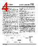
4 / 9 page  24LC256 256K I 2CTM CMOS Serial EEPROM www.artschip.com 4 2.0 PIN DESCRIPTIONS 2.1 A0,A1,A2 Chip Address Inputs The A0, A1,A2 inputs are used by the 24XX256 for multiple device operation. The levels on these inputs are compared with the corresponding bits in the slave address. The chip is selected if the compare is true. Up to eight device may be connected to the same bus by using different chip select bit combinations. If left unconnected, these inputs will be pulled down internally to Vss. 2.2 SDA Serial Data This is a bi-directional pin used to transfer addresses and data into and data out of the device. It is an opendrain terminal, therefore, the SDA bus requires a pull up resistor to Vcc (typical 10 kΩ for 100kHz,2kΩ for 400kHz) For normal data transfer SDA is allowed to change only during SCL low. Changes during SCL high are reserved for indicating the START and STOP conditions. 2.3 SCL Serial Clock This input is used to synchronize the data transfer from and to the device. 2.4 WP This pin can be connected to either Vss, Vcc or left floating. An internal pull-down on this pin will keep the device in the unprotected state if left floating. If tied to Vss or left floating, normal memory operation is enabled (read/write the entire memory 0000-7FFF). If tied to Vcc, WRITE operations are inhibited. Read operations are not affected. 3.0 FUNCTIONAL DESCRIPTION The 24xx256 supports a bi-directional 2-wire bus and data transmission protocol. A device that sends data onto the bus is defined as a transmitter, and a device receiving data as a receiver. The bus must be controlled by a master device which generates the serial clock (SCL), controls the bus access, and generates the START and STOP conditions while the 24xx256 works as a slave. Both master and slave can operate as a transmitter or receiver, but the master device determines which mode is activated. 4.0 BUS CHARACTERISTICS The following bus protocol has been defined: .Data transfer may be initiated only when the bus is not busy. .During data transfer, the data line must remain stable whenever the clock line is HIGH. Changes in the data line while the clock line is HIGH will be interpreted as a START or STOP condition. Accordingly, the following bus conditions have been defined (Figure 4-1). 4.1 Bus not Busy (A) Both data and clock lines remain HIGH. 4.2 Start Data Transfer (B) A HIGH to LOW transition of the SDA line while the clock (SCL) is HIGH determines a START condition. All commands must be preceded by a START condition. 4.3 Stop Data Transfer (C) A Low to HIGH transition of the SDA line while the clock (SCL) is HIGH determines a STOP condition. All operations must end with a STOP condition. 4.4 Data Valid (D) The state of the data line represents valid data when, after a START condition, the data line is stable for the duration of the HIGH period of the clock signal. The data on the line must be changed during the LOW period of the clock signal. There is one bit of data per clock pulse. Each data transfer is initiated with a START condition and terminated with a STOP condition. The number of the data bytes transferred between the START and STOP conditions is determined by the master device. 4.5 Acknowledge Each receiving device, when addressed, is obliged to generate an acknowledge signal after the reception of each byte. The master device must generate an extra clock pulse which is associated with this acknowledge bit. Note: The 24xx256 does not generate any acknowledge bits if an internal programming cycle is in progress. A device that acknowledges must pull down the SDA line during the acknowledge clock pulse in such a way that the SDA line is stable LOW during the HIGH period of the acknowledge related clock pulse. Of course, setup and hold times must be taken into account. During reads, a master must signal an end of data to the slave by NOT generating an acknowledge bit on the last byte that has been clocked out of the slave. In this case, the slave (24xx256) will leave the data line HIGH to enable the master to generate the STOP condition. FIGURE 4-1: DATA TRANSFER SEQUENCE ON THE SERIAL BUS |
|
|
リンク URL |
| ALLDATASHEETはお客様のビジネスに役立ちますか? [ DONATE ] |
Alldatasheetは | 広告 | お問い合わせ | プライバシーポリシー | データシートへのリンク | リンク交換 | メーカーリスト All Rights Reserved©Alldatasheet.com |
| Russian : Alldatasheetru.com | Korean : Alldatasheet.co.kr | Spanish : Alldatasheet.es | French : Alldatasheet.fr | Italian : Alldatasheetit.com Portuguese : Alldatasheetpt.com | Polish : Alldatasheet.pl | Vietnamese : Alldatasheet.vn Indian : Alldatasheet.in | Mexican : Alldatasheet.com.mx | British : Alldatasheet.co.uk | New Zealand : Alldatasheet.co.nz |
|
Family Site : ic2ic.com |
icmetro.com |
 Japanese ▼
 English
 Chinese
 German
 Japanese
 Russian
 Korean
 Spanish
 French
 Italian
 Portuguese
 Polish
 Vietnamese
 Indian
 Mexican
 British
 New Zealand