|
データシートサーチシステム |
|
|
データシートサーチシステム |
|
AD7912AUJ-R2 データシート(PDF) 25 Page - Analog Devices |
|
|
|||||||||||||||||||||||||||||
AD7912AUJ-R2 データシート(HTML) 25 Page - Analog Devices |
|
|
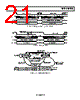
25 / 32 page  AD7912/AD7922 Rev. 0 | Page 25 of 32 SERIAL INTERFACE Figure 37 and Figure 38 show the detailed timing diagrams for serial interfacing to the AD7922 and AD7912, respectively. The serial clock provides the conversion clock and also controls the transfer of information from the AD7912/AD7922 during conversion. The CS signal initiates the data transfer and conversion process. The falling edge of CS puts the track-and-hold into hold mode, takes the bus out of three-state. The analog input is sampled at this point and the conversion is initiated. For the AD7922, the conversion requires 16 SCLK cycles to complete. Once 13 SCLK falling edges have elapsed, the track- and-hold goes back into track on the next SCLK rising edge, as shown in Figure 37 at Point B. On the 16th SCLK falling edge, the DOUT line goes back into three-state. If the rising edge of CS occurs before 16 SCLKs have elapsed, then the conversion is terminated and the DOUT line goes back into three-state. Otherwise, DOUT returns to three-state on the 16th SCLK falling edge, as shown in Figure 37. Sixteen serial clock cycles are required to perform the conversion process and to access data from the AD7922. For the AD7912, the conversion requires 14 SCLK cycles to complete. Once 13 SCLK falling edges have elapsed, the track- and-hold goes back into track on the next SCLK rising edge, as shown in Figure 38 at Point B. If the rising edge of CS occurs before 14 SCLKs have elapsed, then the conversion is terminated and the DOUT line goes back into three-state. If 16 SCLKs are considered in the cycle, DOUT returns to three-state on the 16th SCLK falling edge, as shown in Figure 38. CS going low clocks out the first leading zero to be read in by the microcontroller or DSP. The remaining data is then clocked out by subsequent SCLK falling edges beginning with the second leading zero. Therefore, the first falling clock edge on the serial clock has the first leading zero provided and also clocks out the second leading zero. The final bit in the data transfer is valid on the 16th falling edge, having been clocked out on the previous (15th) falling edge. In applications with a slower SCLK, it is possible to read in data on each SCLK rising edge. In that case, the first falling edge of SCLK clocks out the second leading zero and it can be read in the first rising edge. However, the first leading zero that is clocked out when CS goes low is missed, unless it is read on the first falling SCLK edge. The 15th falling edge of SCLK clocks out the last bit and it can be read in the 15th rising SCLK edge. If CS goes low just after the SCLK falling edge has elapsed, CS clocks out the first leading zero as before and it can be read in the SCLK rising edge. The next SCLK falling edge clocks out the second leading zero and it can be read in the following rising edge. ZERO X 12 34 5 13 14 15 16 X CHN STY X X X X X CHN MOD DB11 DB10 DB2 DB1 DB0 Z t2 t6 t4 t8 t9 t3 t7 t5 t10 t1 tQUIET tCONVERT SCLK CS DOUT THREE-STATE THREE-STATE DIN B Figure 37. AD7922 Serial Interface Timing Diagram ZERO X 12 34 5 13 14 15 16 X CHN STY X X X X X CHN MOD DB9 DB8 DB0 ZERO ZERO Z t2 t6 t4 t8 t9 t3 t7 t5 t10 t1 tQUIET tCONVERT SCLK CS DOUT THREE-STATE THREE-STATE TWO TRAILING ZEROS DIN B Figure 38. AD7912 Serial Interface Timing Diagram |
|
リンク URL |
| ALLDATASHEETはお客様のビジネスに役立ちますか? [ DONATE ] |
Alldatasheetは | 広告 | お問い合わせ | プライバシーポリシー | データシートへのリンク | リンク交換 | メーカーリスト All Rights Reserved©Alldatasheet.com |
| Russian : Alldatasheetru.com | Korean : Alldatasheet.co.kr | Spanish : Alldatasheet.es | French : Alldatasheet.fr | Italian : Alldatasheetit.com Portuguese : Alldatasheetpt.com | Polish : Alldatasheet.pl | Vietnamese : Alldatasheet.vn Indian : Alldatasheet.in | Mexican : Alldatasheet.com.mx | British : Alldatasheet.co.uk | New Zealand : Alldatasheet.co.nz |
|
Family Site : ic2ic.com |
icmetro.com |
 Japanese ▼
 English
 Chinese
 German
 Japanese
 Russian
 Korean
 Spanish
 French
 Italian
 Portuguese
 Polish
 Vietnamese
 Indian
 Mexican
 British
 New Zealand