|
データシートサーチシステム |
|
|
データシートサーチシステム |
|
LYT7503 データシート(PDF) 3 Page - Power Integrations, Inc. |
|
|
|||||||||||||||||||||||||||||
LYT7503 データシート(HTML) 3 Page - Power Integrations, Inc. |
|
|
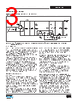
3 / 12 page  Rev. C 07/16 3 LYT7503-7504 www.power.com Figure 5. Schematic from DER-561 7.5 W, 60 V, 125 mA Dimmable Non-Isolated A19 LED Driver for Wide Input Range: 90 – 300 V VAC using LYT7503D in Low-Side Buck Configuration. Applications Design Example DER-561 a Low-Line Dimmable 7.5 W, Wide Input, High Power factor LED Bulb Driver. Circuit Description The circuit shown in Figure 5 is a LED driver configured as a low-side buck utilizing the LYT7503D from the LYTSwitch-7 family of ICs. This is a low component count (20 parts) dimmable LED driver designed to power a 60 V LED voltage string at 125 mA output current from an input voltage of 90 VAC to 300 VAC. Dimming performance is optimized at low-line input (i.e. 120 VAC), while maintaining accurate regulation for non-dimmable high-line input. LYTSwitch-7 is a SO-8 package LED driver IC family designed for non-isolated buck applications. The LYTSwitch-7 family provides high efficiency, high power factor and accurate LED current regulation. It incorporates a high-voltage 725 V power MOSFET and a control engine to switch the MOSFET in critical conduction mode (CM) with variable on-time and variable frequency which also helps achieve low EMI, and low THD. The controller also integrates protection features such as input and output overvoltage protection, thermal fold-back, over-temperature shutdown, output short-circuit and over-current protection. The controller also allows natural dimming with only the addition of a damper resistor and an RC network for damping the input current ringing when the TRIAC turns on. Key Design Considerations Input Stage The input fusible resistor RF1 provides multiple-purpose function – safety protection, current limiting against differential surge and acts as a damping element reducing inrush-current ringing when TRIAC dimming. Varistor RV1 acts as a voltage clamp that limits the voltage spike on the primary during line transients and surge events. A 250 VAC rated part was selected with a maximum clamping voltage specification of 710 VDC – lower than the device Drain voltage (725 V). The AC input voltage is full wave rectified by BR1 to achieve good power factor and low THD. The rectified AC supply is filtered by the input capacitors C1 and C2. Too much capacitance degrades power factor and THD, so the values of the input capacitors were set to the minimum necessary to meet EMI (with suitable margin). Inductor L1, C1 and C2 form a π (pi) filter, which attenuates conducted differential and common mode EMI currents. If required a ≥10 kΩ resistor (not shown) can be added across L1 to damp the Q-factor of the filter inductor to improve the filtering of high frequency EMI without reducing low frequency attenuation. The addition of the RC damper network R2 and C3 makes the driver compatible with TRAIC (phase-cut) dimmers. The RC damper in the circuit may be placed before or after the bridge rectifier. In this design, the RC damper is located after the bridge rectifier for higher dimming range. Putting the RC damper before the bridge would load the TRIAC dimmer and maintain full output to a lower conduction angle but would result in reduced dimming range. LYTSwitch-7 Controller Stage The LED driver circuit is a low-side buck configuration operating in critical conduction mode; the controller allows complete transfer of the energy stored in the inductor to the load before starting the next switch cycle. The inductor demagnetization is sensed, detecting when the voltage across the inductor begins to collapse (towards zero) as flywheel diode (D1) conduction ceases. Capacitor C4 provides local decoupling for the BYPASS (BP) pin IC and provides power to the LYTSwitch-7 controller during the MOSFET on-time. The IC has an internal regulator that draws power from the high-voltage DRAIN (D) pin and charges the bypass capacitor C4 during the power switch off-time. The typical BYPASS pin voltage is 5.22 V. To keep the IC operating normally (especially during the dead time), where V IN < VOUT, and during dimming at low conduction angles, resistors R6 and R10 are employed to keep the bypass capacitor charged. The value of the bypass capacitor should be large enough to keep the bypass voltage above the V BP(RESET) reset value of 4.5 V. The suggested minimum value for the bypass capacitor is 10 µF; an X7R type is recommended if using a ceramic type capacitor. Constant output current regulation is achieved through the FEED- BACK (FB) pin directly sensing the DRAIN pin current during the MOSFET on-time via external current sense resistors (RFB) R3 and PI-8023-071416 LYTSwitch-7 U1 LYT7503D D S R8 100 kΩ R10 51 kΩ R6 51 kΩ R2 510 Ω 2 W L N RTN 60 V, 125 mA +V D1 US1J-13-F L1 4.7 mH T1 EE10 4 6 BR1 B10S-G 1000 V R3 0.68 Ω 1% 1/3 W RV1 275 VAC R1 47 Ω 2 W R4 51.1 Ω 1%, 1/8 W R9 402 kΩ 1% R5 12.4 kΩ 1% 1/8 W C1 22 nF 450 V C2 120 nF 450 V C3 220 nF 450 V C6 220 µF 80 V C5 100 pF 1000 V C4 10 µF 10 V FB M BP 90 - 300 VAC |
|
|
リンク URL |
| ALLDATASHEETはお客様のビジネスに役立ちますか? [ DONATE ] |
Alldatasheetは | 広告 | お問い合わせ | プライバシーポリシー | データシートへのリンク | リンク交換 | メーカーリスト All Rights Reserved©Alldatasheet.com |
| Russian : Alldatasheetru.com | Korean : Alldatasheet.co.kr | Spanish : Alldatasheet.es | French : Alldatasheet.fr | Italian : Alldatasheetit.com Portuguese : Alldatasheetpt.com | Polish : Alldatasheet.pl | Vietnamese : Alldatasheet.vn Indian : Alldatasheet.in | Mexican : Alldatasheet.com.mx | British : Alldatasheet.co.uk | New Zealand : Alldatasheet.co.nz |
|
Family Site : ic2ic.com |
icmetro.com |
 Japanese ▼
 English
 Chinese
 German
 Japanese
 Russian
 Korean
 Spanish
 French
 Italian
 Portuguese
 Polish
 Vietnamese
 Indian
 Mexican
 British
 New Zealand