|
データシートサーチシステム |
|
|
データシートサーチシステム |
|
LYT7503 データシート(PDF) 6 Page - Power Integrations, Inc. |
|
|
|||||||||||||||||||||||||||||
LYT7503 データシート(HTML) 6 Page - Power Integrations, Inc. |
|
|
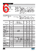
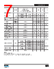
6 / 12 page  Rev. C 07/16 6 LYT7503-7504 www.power.com Absolute Maximum Ratings(1,3) DRAIN Pin Voltage: LYT750x ........................... -0.3 V to 725 V DRAIN Pin Peak Current: LYT7503 ...........................1.05 A (1.3 A)(1) LYT7504 .............................2.1 A (2.6 A)(1) BYPASS Pin Voltage ...................................................-0.3 V to 6.0 V MULTIFUNCTION, FEEDBACK Pin Voltage................ -0.45 V to 7.0 V(2) Lead Temperature ................................................................ 260 °C Storage Temperature ...................................................-65 to 150 °C Operating Junction Temperature................................ -40 to 150 °C(4) Notes: 1. The higher peak Drain current (in parentheses) is allowed while the Drain-Source voltage is simultaneously less than 400 V for the integrated MOSFET. 2. If the SOURCE pin is open circuit, -0.7 V between FEEDBACK pin and SOURCE pin is observed with no degradation in performance. 3. The absolute maximum ratings specified may be applied one at a time without causing permanent damage to the product. Exposure to absolute maximum ratings for extended periods of time may affect product reliability. 4. Normally limited by internal circuitry. Parameter Symbol Conditions SOURCE = 0 V T J = -40 °C to 125 °C (Unless Otherwise Specified) Min Typ Max Units Control Functions Minimum Switching Frequency f MIN 18 20 22 kHz Maximum Switch ON-Time T ON(MAX) 10 µs Minimum Switch ON-Time T ON(MIN) 1.012 1.1 1.25 µs FEEDBACK Pin Reference Voltage V FB(REF) T J = 25 °C See Note C -285 -279 -273 mV Dead Zone Detect Threshold V TH(DZ) 0.3 × V FB(REF) V Maximum Constant Current Zone T CC(MAX) 6 ms Forced Minimum Constant Current Zone T CC(MIN) 1.2 ms BYPASS Pin Supply Current I SBY Standby (MOSFET not switching) 180 µA I DSS MOSFET Switching LYT7503 785 µA LYT7504 850 BYPASS Pin Charge Current I CH1 V BP = 0.0 V, VDS ≥ 36 V -10 -4.5 mA I CH2 V BP = 5.0 V, VDS ≥ 36 V -6 -2 mA BYPASS Pin Voltage V BP 5.075 5.22 5.35 V BYPASS Pin Shunt Voltage V BP(SHUNT) 5.2 5.39 5.55 V BYPASS Pin Power-Up Reset Threshold Voltage V BP(RESET) 4.35 4.5 4.65 V Thermal Resistance Thermal Resistance: SO-8 Package: (q JA)................................100 °C/W (2) , 80 °C/W(3) (q JC) (1) ................................................ 30 °C/W Notes: 1. Measured on the SOURCE pin close to plastic interface. 2. Soldered to 0.36 sq. inch (232 mm2) 2 oz. (610 g/m2) copper clad pcb, with no external heat sink attached. 3. Soldered to 1 sq. in. (645 mm2), 2 oz, (610 g/m2) copper clad pcb. |
|
|
リンク URL |
| ALLDATASHEETはお客様のビジネスに役立ちますか? [ DONATE ] |
Alldatasheetは | 広告 | お問い合わせ | プライバシーポリシー | データシートへのリンク | リンク交換 | メーカーリスト All Rights Reserved©Alldatasheet.com |
| Russian : Alldatasheetru.com | Korean : Alldatasheet.co.kr | Spanish : Alldatasheet.es | French : Alldatasheet.fr | Italian : Alldatasheetit.com Portuguese : Alldatasheetpt.com | Polish : Alldatasheet.pl | Vietnamese : Alldatasheet.vn Indian : Alldatasheet.in | Mexican : Alldatasheet.com.mx | British : Alldatasheet.co.uk | New Zealand : Alldatasheet.co.nz |
|
Family Site : ic2ic.com |
icmetro.com |
 Japanese ▼
 English
 Chinese
 German
 Japanese
 Russian
 Korean
 Spanish
 French
 Italian
 Portuguese
 Polish
 Vietnamese
 Indian
 Mexican
 British
 New Zealand