|
データシートサーチシステム |
|
|
データシートサーチシステム |
|
ADL5385ACPZ-R7 データシート(PDF) 16 Page - Analog Devices |
|
|
|||||||||||||||||||||||||||||
ADL5385ACPZ-R7 データシート(HTML) 16 Page - Analog Devices |
|
|
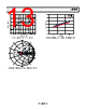
16 / 24 page  ADL5385 Data Sheet Rev. D | Page 16 of 24 OPTIMIZATION The carrier feedthrough and sideband suppression performance of the ADL5385 can be improved through the use of optimization techniques. Carrier Feedthrough Nulling Carrier feedthrough results from minute dc offsets that occur between each of the differential baseband inputs. In an ideal modulator, the quantities (VIOPP − VIOPN) and (VQOPP − VQOPN) are equal to zero, and this results in no carrier feedthrough. In a real modulator, those two quantities are nonzero and, when mixed with the LO, result in a finite amount of carrier feedthrough. The ADL5385 is designed to provide a minimal amount of carrier feedthrough. If even lower carrier feedthrough levels are required, minor adjustments can be made to the (VIOPP − VIOPN) and (VQOPP − VQOPN) offsets. The I-channel offset is held constant while the Q-channel offset is varied until a minimum carrier feedthrough level is obtained. The Q-channel offset required to achieve this minimum is held constant while the offset on the I-channel is adjusted, until a better minimum is reached. Through two iterations of this process, the carrier feedthrough can be reduced to as low as the output noise. The ability to null is sometimes limited by the resolution of the offset adjustment. Figure 30 shows the relationship of carrier feedthrough vs. dc offset. –58 –94 VP-VN OFFEST (µV) –62 –66 –70 –74 –78 –82 –86 –90 Figure 30. Carrier Feedthrough vs. DC Offset Voltage at 450 MHz Note that throughout the nulling process, the dc bias for the baseband inputs remains at 500 mV. When no offset is applied, VIOPP = VIOPN = 500 mV, or VIOPP − VIOPN = VIOS = 0 V When an offset of +VIOS is applied to the I-channel inputs, VIOPP = 500 mV + VIOS/2, while VIOPN = 500 mV − VIOS/2, such that VIOPP − VIOPN = VIOS The same applies to the Q channel. It is often desirable to perform a one-time carrier null calibration. This is usually performed at a single frequency. Figure 31 shows how carrier feedthrough varies with LO frequency over a range of ±50 MHz on either side of a null at 350 MHz. –25 –85 310 400 OUTPUT FREQUENCY (MHz) –30 –35 –40 –45 –50 –55 –60 –65 –70 –75 –80 320 330 340 350 360 370 380 390 300 Figure 31. Carrier Feedthrough vs. Frequency After Nulling at 350 MHz Sideband Suppression Optimization Sideband suppression results from relative gain and relative phase offsets between the I and Q channels and can be suppressed through adjustments to those two parameters. Figure 32 illustrates how sideband suppression is affected by the gain and phase imbalances. 0dB 0.0125dB 0.025dB 0.05dB 0.125dB 0.25dB 0.5dB 1.25dB 2.5dB 0 –10 –20 –30 –40 –50 –60 –70 –80 –90 0.01 0.1 1 10 100 PHASE ERROR (Degrees) Figure 32. Sideband Suppression vs. Quadrature Phase Error for Various Quadrature Amplitude Offsets Figure 32 underscores the fact that adjusting one parameter improves the sideband suppression only to a point; the other parameter must also be adjusted. For example, if the amplitude offset is 0.25 dB, improving the phase imbalance better than 1° does not yield any improvement in the sideband suppression. For optimum sideband suppression, an iterative adjustment between phase and amplitude is required. The sideband suppression nulling can be performed either through adjusting the gain for each channel or through the modification of the phase and gain of the digital data coming from the digital signal processor. |
|
|
リンク URL |
| ALLDATASHEETはお客様のビジネスに役立ちますか? [ DONATE ] |
Alldatasheetは | 広告 | お問い合わせ | プライバシーポリシー | データシートへのリンク | リンク交換 | メーカーリスト All Rights Reserved©Alldatasheet.com |
| Russian : Alldatasheetru.com | Korean : Alldatasheet.co.kr | Spanish : Alldatasheet.es | French : Alldatasheet.fr | Italian : Alldatasheetit.com Portuguese : Alldatasheetpt.com | Polish : Alldatasheet.pl | Vietnamese : Alldatasheet.vn Indian : Alldatasheet.in | Mexican : Alldatasheet.com.mx | British : Alldatasheet.co.uk | New Zealand : Alldatasheet.co.nz |
|
Family Site : ic2ic.com |
icmetro.com |
 Japanese ▼
 English
 Chinese
 German
 Japanese
 Russian
 Korean
 Spanish
 French
 Italian
 Portuguese
 Polish
 Vietnamese
 Indian
 Mexican
 British
 New Zealand