|
データシートサーチシステム |
|
|
データシートサーチシステム |
|
WM8196 データシート(PDF) 14 Page - Cirrus Logic |
|
|
|||||||||||||||||||||||||||||
WM8196 データシート(HTML) 14 Page - Cirrus Logic |
|
|
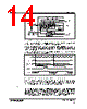
14 / 32 page  WM8196 Production Data w PD Rev 4.6 October 2008 14 TIMING CONTROL S/H 4-BIT RLC DAC CL + + - TO OFFSET DAC RLC CDS FROM CONTROL INTERFACE S/H V S R S FROM CONTROL INTERFACE MCLK VSMP RLC/ACYC INPUT SAMPLING BLOCK FOR RED CHANNEL CDS C IN RINP VRLC/ VBIAS 2 1 EXTERNAL VRLC VRLCEXT Figure 9 Reset Level Clamping and CDS Circuitry If auto-cycling is not required, RLC can be selected by pin RLC/ACYC. Figure 10 illustrates control of RLC for a typical CCD waveform, with CL applied during the reset period. The input signal applied to the RLC/ACYC pin is sampled on the positive edge of MCLK that occurs during each VSMP pulse. The sampled level, high (or low) controls the presence (or absence) of the internal CL pulse on the next reset level. The position of CL can be adjusted by using control bits CDSREF[1:0] (Figure 11). If auto-cycling is required, pin RLC/ACYC is no longer available for this function and control bit RLCINT determines whether clamping is applied. Figure 10 Relationship of RLC Pin, MCLK and VSMP to Internal Clamp Pulse, CL The VRLC/VBIAS pin can be driven internally by a 4-bit DAC (RLCDAC) by writing to control bits RLCV[3:0]. The RLCDAC range and step size may be increased by writing to control bit RLCDACRNG. Alternatively, the VRLC/VBIAS pin can be driven externally by writing to control bit VRLCEXT to disable the RLCDAC and then applying a d.c. voltage to the pin. CDS/NON-CDS PROCESSING For CCD type input signals, the signal may be processed using CDS, which will remove pixel-by-pixel common mode noise. For CDS operation, the video level is processed with respect to the video reset level, regardless of whether RLC has been performed. To sample using CDS, control bit CDS must be set to 1 (default), this sets switch 2 into the position shown in Figure 9 and causes the signal reference to come from the video reset level. The time at which the reset level is sampled, by clock Rs/CL, is adjustable by programming control bits CDSREF[1:0], as shown in Figure 11. MCLK VSMP ACYC/RLC or RLCINT CL (CDSREF = 01) INPUT VIDEO 1X X 0 X X 0 RGB RGB No RLC on this Pixel RLC on this Pixel Programmable Delay RGB |
|
リンク URL |
| ALLDATASHEETはお客様のビジネスに役立ちますか? [ DONATE ] |
Alldatasheetは | 広告 | お問い合わせ | プライバシーポリシー | データシートへのリンク | リンク交換 | メーカーリスト All Rights Reserved©Alldatasheet.com |
| Russian : Alldatasheetru.com | Korean : Alldatasheet.co.kr | Spanish : Alldatasheet.es | French : Alldatasheet.fr | Italian : Alldatasheetit.com Portuguese : Alldatasheetpt.com | Polish : Alldatasheet.pl | Vietnamese : Alldatasheet.vn Indian : Alldatasheet.in | Mexican : Alldatasheet.com.mx | British : Alldatasheet.co.uk | New Zealand : Alldatasheet.co.nz |
|
Family Site : ic2ic.com |
icmetro.com |
 Japanese ▼
 English
 Chinese
 German
 Japanese
 Russian
 Korean
 Spanish
 French
 Italian
 Portuguese
 Polish
 Vietnamese
 Indian
 Mexican
 British
 New Zealand