|
データシートサーチシステム |
|
|
データシートサーチシステム |
|
WM8196 データシート(PDF) 18 Page - Cirrus Logic |
|
|
|||||||||||||||||||||||||||||
WM8196 データシート(HTML) 18 Page - Cirrus Logic |
|
|
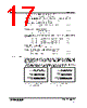
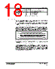
18 / 32 page  WM8196 Production Data w PD Rev 4.6 October 2008 18 OUTPUT FORMAT MUXOP[1:0] OUTPUT PINS OUTPUT 8+8-bit multiplexed 00, 01, 10 OP[7:0] A = d15, d14, d13, d12, d11, d10, d9, d8 B = d7, d6, d5, d4, d3, d2, d1,d0 4+4+4+4-bit (nibble) 11 OP[7:4] A = d15, d14, d13, d12 B = d11, d10, d9, d8 C = d7, d6, d5, d4 D = d3, d2, d1, d0 Table 2 Details of Output Data Shown in Figure 15 and Figure 16. CONTROL INTERFACE The internal control registers are programmable via the serial digital control interface. The register contents can be read back via the serial interface on pin OP[7]/SDO. Note: It is recommended that a software reset is carried out after the power-up sequence, before writing to any other register. This ensures that all registers are set to their default values (as shown in Table 6). SERIAL INTERFACE: REGISTER WRITE Figure 17 shows register writing in serial mode. Three pins, SCK, SDI and SEN are used. A six-bit address (a5, 0, a3, a2, a1, a0) is clocked in through SDI, MSB first, followed by an eight-bit data word (b7, b6, b5, b4, b3, b2, b1, b0), also MSB first. Each bit is latched on the rising edge of SCK. When the data has been shifted into the device, a pulse is applied to SEN to transfer the data to the appropriate internal register. Note all valid registers have address bit a4 equal to 0 in write mode. SCK SEN SDI a5 0 a3a2a1 a0b7b6b5 b4b3b2b1b0 Address Data Word Figure 17 Serial Interface Register Write A software reset is carried out by writing to Address “000100” with any value of data, i.e. Data Word = XXXXXXXX. SERIAL INTERFACE: REGISTER READ-BACK Figure 18 shows register read-back in serial mode. Read-back is initiated by writing to the serial bus as described above but with address bit a4 set to 1, followed by an 8-bit dummy data word. Writing address (a5, 1, a3, a2, a1, a0) will cause the contents (d7, d6, d5, d4, d3, d2, d1, d0) of corresponding register (a5, 0, a3, a2, a1, a0) to be output MSB first on pin SDO (on the falling edge of SCK). Note that pin SDO is shared with an output pin, OP[7], therefore OEB should always be held low when register read-back data is expected on this pin. The next word may be read in to SDI while the previous word is still being output on SDO. |
|
リンク URL |
| ALLDATASHEETはお客様のビジネスに役立ちますか? [ DONATE ] |
Alldatasheetは | 広告 | お問い合わせ | プライバシーポリシー | データシートへのリンク | リンク交換 | メーカーリスト All Rights Reserved©Alldatasheet.com |
| Russian : Alldatasheetru.com | Korean : Alldatasheet.co.kr | Spanish : Alldatasheet.es | French : Alldatasheet.fr | Italian : Alldatasheetit.com Portuguese : Alldatasheetpt.com | Polish : Alldatasheet.pl | Vietnamese : Alldatasheet.vn Indian : Alldatasheet.in | Mexican : Alldatasheet.com.mx | British : Alldatasheet.co.uk | New Zealand : Alldatasheet.co.nz |
|
Family Site : ic2ic.com |
icmetro.com |
 Japanese ▼
 English
 Chinese
 German
 Japanese
 Russian
 Korean
 Spanish
 French
 Italian
 Portuguese
 Polish
 Vietnamese
 Indian
 Mexican
 British
 New Zealand