|
データシートサーチシステム |
|
|
データシートサーチシステム |
|
WM8196 データシート(PDF) 20 Page - Cirrus Logic |
|
|
|||||||||||||||||||||||||||||
WM8196 データシート(HTML) 20 Page - Cirrus Logic |
|
|
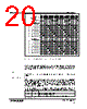
20 / 32 page  WM8196 Production Data w PD Rev 4.6 October 2008 20 MCLK VSMP (VDEL = 000) INTVSMP POSNNEG = 1 (VDEL = 001) INTVSMP (VDEL = 010) INTVSMP (VDEL = 011) INTVSMP (VDEL = 100) INTVSMP (VDEL = 101) INTVSMP (VDEL = 110) INTVSMP (VDEL = 111) INTVSMP POSNNEG = 0 (VDEL = 000) INTVSMP (VDEL = 001) INTVSMP (VDEL = 010) INTVSMP (VDEL = 011) INTVSMP (VDEL = 100) INTVSMP (VDEL = 101) INTVSMP (VDEL = 110) INTVSMP (VDEL = 111) INTVSMP INPUT PINS V S V S V S V S V S V S V S V S V S V S V S V S V S V S V S V S V S V S V S V S V S V S V S V S V S V S V S V S V S V S V S V S V S V S V S V S V S V S V S V S V S V S V S V S V S V S V S V S Figure 19 Internal VSMP Pulses Generated by Programmable VSMP Detect Circuit REFERENCES The ADC reference voltages are derived from an internal bandgap reference, and buffered to pins VRT and VRB, where they must be decoupled to ground. Pin VRX is driven by a similar buffer, and also requires decoupling. The output buffer from the RLCDAC also requires decoupling at pin VRLC/VBIAS POWER SUPPLY The WM8196 can run from a 5V single supply or from split 5V (core) and 3.3V (digital interface) supplies. POWER MANAGEMENT Power management for the device is performed via the Control Interface. The device can be powered on or off completely setting by the EN bit and SELPD bit low. Alternatively, when control bit SELPD is high, only blocks selected by further control bits (SELDIS[3:0]) are powered down. This allows the user to optimise power dissipation in certain modes, or to define an intermediate standby mode to allow a quicker recovery into a fully active state. In Line-by-line operation, the green and blue channel PGAs are automatically powered down. All the internal registers maintain their previously programmed value in power down modes and the Control Interface inputs remain active. Table 3 summarises the power down control bit functions. EN SELDPD 0 0 Device completely powers down. 1 0 Device completely powers up. X 1 Blocks with respective SELDIS[3:0] bit high are disabled. Table 3 Power Down Control |
|
リンク URL |
| ALLDATASHEETはお客様のビジネスに役立ちますか? [ DONATE ] |
Alldatasheetは | 広告 | お問い合わせ | プライバシーポリシー | データシートへのリンク | リンク交換 | メーカーリスト All Rights Reserved©Alldatasheet.com |
| Russian : Alldatasheetru.com | Korean : Alldatasheet.co.kr | Spanish : Alldatasheet.es | French : Alldatasheet.fr | Italian : Alldatasheetit.com Portuguese : Alldatasheetpt.com | Polish : Alldatasheet.pl | Vietnamese : Alldatasheet.vn Indian : Alldatasheet.in | Mexican : Alldatasheet.com.mx | British : Alldatasheet.co.uk | New Zealand : Alldatasheet.co.nz |
|
Family Site : ic2ic.com |
icmetro.com |
 Japanese ▼
 English
 Chinese
 German
 Japanese
 Russian
 Korean
 Spanish
 French
 Italian
 Portuguese
 Polish
 Vietnamese
 Indian
 Mexican
 British
 New Zealand