 |
データシートサーチシステム |
|
|
データシートサーチシステム |
|
The question interval is too short.
Please try again in a few seconds.

Hello, Please ask a question about GD25LE256DFJS Datasheet
# Example questions:
➢ Explain how the block protect (bp4-bp0) bits and the cmp bit interact to define the protected memory area. provide an example scenario where cmp=0 and another where cmp=1 and how the protected area differs.
➢ What does the wip (write in progress) bit in the status register indicate, and why is it important to check this bit before issuing another program, erase, or write status register command?
➢ Describe the differences between software protection, hardware protection, and power supply lock-down modes for the status register, referencing the srp1 and srp0 bits and the wp# pin.
| Part No. | GD25LE256DFJS |
| Manufacturer | GIGADEVICE |
| Size | 1Mb |
| Pages | 83 pages |
| Description | 1.8V Uniform Sector Dual and Quad Serial Flash |


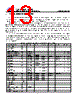


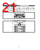


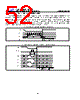


Okay, let's break down the information provided in the GD25LE256D datasheet excerpt. Here's a summary, organized for clarity.
1. Device Overview:
️· This excerpt covers a serial flash memory device (GD25LE256D).
️· It focuses on capabilities and limitations related to programming, erasing, and status register control.
2. Key Features & Concepts:
️· Write in Progress (WIP): A status bit. `1` means the device is busy with a program, erase, or write operation. `0` means it's idle and ready.
️· Write Enable Latch (WEL): A status bit. `1` enables write operations (Write Status Register, Program, Erase). `0` disables them. You need `WEL = 1` before you can write.
️· Block Protect (BP4-BP0): Non-volatile bits (they retain their value even when power is removed). These define a software-protected area. When set, these bits prevent Program and Erase commands from affecting the corresponding memory blocks. This provides a way to protect certain sections of the memory from accidental modification.
️· Status Register Protection (SRP1, SRP0): Non-volatile bits that control how the Status Register itself can be modified. They implement different protection modes:
- Software Protection (Default): The Status Register can be written to after a Write Enable command.
- Hardware Protection: The Status Register is locked by asserting the `#WP` pin (typically an external pin connected to ground or high).
- Power Supply Lock-Down: The Status Register is permanently locked until a power cycle.
- One-Time Programmable (OTP): The Status Register is permanently locked after a single write operation.
️· CMP (Compare Bit): This bit is used in conjunction with the BP bits to determine the memory area that is protected.
3. Tables of Interest:
️· Table 1: Protected Area Size (CMP=0 and CMP=1): This table defines how the BP bits (BP4-BP0) relate to the size and location of the software-protected memory blocks. The meaning of the BP bits changes based on the value of the CMP bit.
️· Status Register Table: This table defines all status and control bits in the Status Register, along with their functions and how they interact.
4. Important Considerations/Key Takeaways:
️· WEL is Crucial: You *must* have `WEL = 1` before attempting any Write Status Register, Program, or Erase commands.
️· CMP and BP bits determine protection: The actual memory regions that are protected depend on the `CMP` bit and the combination of `BP` bits. Refer to Table 1 to understand the specific mapping.
️· SRP Offers Multiple Protection Levels: The SRP bits provide increasing levels of protection for the Status Register itself, from simple software control to permanent locking.
️· External WP Pin: The hardware protection mode relies on an external pin (#WP). Check the device's pinout and associated documentation to determine its purpose.
To help me provide more specific and useful information, could you tell me:
* What are you trying to do with the GD25LE256D? (e.g., writing code, designing a circuit, troubleshooting a problem)
* Are there any particular aspects of the information that you'd like me to elaborate on?
1. Device Overview:
️· This excerpt covers a serial flash memory device (GD25LE256D).
️· It focuses on capabilities and limitations related to programming, erasing, and status register control.
2. Key Features & Concepts:
️· Write in Progress (WIP): A status bit. `1` means the device is busy with a program, erase, or write operation. `0` means it's idle and ready.
️· Write Enable Latch (WEL): A status bit. `1` enables write operations (Write Status Register, Program, Erase). `0` disables them. You need `WEL = 1` before you can write.
️· Block Protect (BP4-BP0): Non-volatile bits (they retain their value even when power is removed). These define a software-protected area. When set, these bits prevent Program and Erase commands from affecting the corresponding memory blocks. This provides a way to protect certain sections of the memory from accidental modification.
️· Status Register Protection (SRP1, SRP0): Non-volatile bits that control how the Status Register itself can be modified. They implement different protection modes:
- Software Protection (Default): The Status Register can be written to after a Write Enable command.
- Hardware Protection: The Status Register is locked by asserting the `#WP` pin (typically an external pin connected to ground or high).
- Power Supply Lock-Down: The Status Register is permanently locked until a power cycle.
- One-Time Programmable (OTP): The Status Register is permanently locked after a single write operation.
️· CMP (Compare Bit): This bit is used in conjunction with the BP bits to determine the memory area that is protected.
3. Tables of Interest:
️· Table 1: Protected Area Size (CMP=0 and CMP=1): This table defines how the BP bits (BP4-BP0) relate to the size and location of the software-protected memory blocks. The meaning of the BP bits changes based on the value of the CMP bit.
️· Status Register Table: This table defines all status and control bits in the Status Register, along with their functions and how they interact.
4. Important Considerations/Key Takeaways:
️· WEL is Crucial: You *must* have `WEL = 1` before attempting any Write Status Register, Program, or Erase commands.
️· CMP and BP bits determine protection: The actual memory regions that are protected depend on the `CMP` bit and the combination of `BP` bits. Refer to Table 1 to understand the specific mapping.
️· SRP Offers Multiple Protection Levels: The SRP bits provide increasing levels of protection for the Status Register itself, from simple software control to permanent locking.
️· External WP Pin: The hardware protection mode relies on an external pin (#WP). Check the device's pinout and associated documentation to determine its purpose.
| Part No. | GD25LE256DFJS |
| Manufacturer | GIGADEVICE |
| Size | 1Mb |
| Pages | 83 pages |
| Description | 1.8V Uniform Sector Dual and Quad Serial Flash |
| ALLDATASHEETはお客様のビジネスに役立ちますか? [ DONATE ] |
Alldatasheetは | 広告 | お問い合わせ | プライバシーポリシー | データシートへのリンク | リンク交換 | メーカーリスト All Rights Reserved©Alldatasheet.com |
| Russian : Alldatasheetru.com | Korean : Alldatasheet.co.kr | Spanish : Alldatasheet.es | French : Alldatasheet.fr | Italian : Alldatasheetit.com Portuguese : Alldatasheetpt.com | Polish : Alldatasheet.pl | Vietnamese : Alldatasheet.vn Indian : Alldatasheet.in | Mexican : Alldatasheet.com.mx | British : Alldatasheet.co.uk | New Zealand : Alldatasheet.co.nz |
|
Family Site : ic2ic.com |
icmetro.com |
 Japanese ▼
  English
 Chinese
 German
 Russian
 Korean
 Spanish
 French
 Italian
 Portuguese
 Polish
 Vietnamese
 Indian
 Mexican
 British
 New Zealand