|
データシートサーチシステム |
|
|
データシートサーチシステム |
|
GD25LE256DFJS データシート(PDF) 22 Page - GigaDevice Semiconductor (Beijing) Inc. |
|
|
|||||||||||||||||||||||||||||
GD25LE256DFJS データシート(HTML) 22 Page - GigaDevice Semiconductor (Beijing) Inc. |
|
|
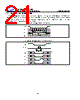
22 / 83 page  1.8V Uniform Sector Dual and Quad Serial Flash GD25LE256D 22 7.5. Write Enable for Volatile Status Register (50H) The non-volatile Status Register bits can also be written to as volatile bits. This gives more flexibility to change the system configuration and memory protection schemes quickly without waiting for the typical non-volatile bit write cycles or affecting the endurance of the Status Register non-volatile bits. The Write Enable for Volatile Status Register command must be issued prior to a Write Status Register command, and any other commands can't be inserted between them. Otherwise, Write Enable for Volatile Status Register will be cleared. The Write Enable for Volatile Status Register command will not set the Write Enable Latch bit, it is only valid for the Write Status Register command to change the volatile Status Register bit values. Figure6. Write Enable for Volatile Status Register Sequence Diagram CS# SCLK Command(50H) SI SO 0 1 2 3 4 5 6 7 High-Z Figure6a. Write Enable for Volatile Status Register Sequence Diagram (QPI) CS# SCLK IO0 IO1 IO2 IO3 0 1 Command 50H |
|
リンク URL |
| ALLDATASHEETはお客様のビジネスに役立ちますか? [ DONATE ] |
Alldatasheetは | 広告 | お問い合わせ | プライバシーポリシー | データシートへのリンク | リンク交換 | メーカーリスト All Rights Reserved©Alldatasheet.com |
| Russian : Alldatasheetru.com | Korean : Alldatasheet.co.kr | Spanish : Alldatasheet.es | French : Alldatasheet.fr | Italian : Alldatasheetit.com Portuguese : Alldatasheetpt.com | Polish : Alldatasheet.pl | Vietnamese : Alldatasheet.vn Indian : Alldatasheet.in | Mexican : Alldatasheet.com.mx | British : Alldatasheet.co.uk | New Zealand : Alldatasheet.co.nz |
|
Family Site : ic2ic.com |
icmetro.com |
 Japanese ▼
 English
 Chinese
 German
 Japanese
 Russian
 Korean
 Spanish
 French
 Italian
 Portuguese
 Polish
 Vietnamese
 Indian
 Mexican
 British
 New Zealand