 |
データシートサーチシステム |
|
|
データシートサーチシステム |
|
The question interval is too short.
Please try again in a few seconds.

Hello, Please ask a question about LM2507 Datasheet
# Example questions:
➢ What is the significance of parameters like 'set up time' and 'hold time' in the context of the i80 cpu interface, and why are these important?
➢ What is the primary function of the idr pin and how does its setting (high or low) affect the read transaction process?
➢ Explain the relationship between the master's clock frequency (clk) and the slave's output timing. how might adjustments to the master's clock frequency be necessary to ensure compatibility with the target device?
| Part No. | LM2507 |
| Manufacturer | NSC |
| Size | 977 Kbytes |
| Pages | 22 pages |
| Description | Low Power Mobile Pixel Link (MPL) Level 0, 16-bit CPU Display interface Serializer and Deserializer |


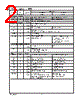

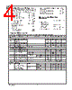

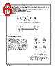
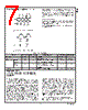



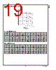
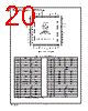


1. General Overview
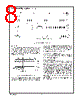
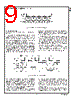
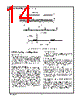
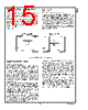
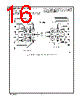
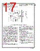
️· Purpose: This document describes the timing and operational details of a communication link (likely a serial interface called MPL) designed for connecting a host (Master) to a peripheral (Slave), potentially for display applications.
️· Goal: To ensure compatibility between the Master and Slave devices regarding timing requirements.
️· Key Feature: Dual Read Operation: Enables consistent behavior regardless of MPL link usage.
2. Timing Parameters & Transactions
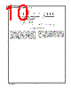
️· WRITE Transaction (i80 CPU Interface):
- Master-Side Timing:
■ T1: Data Setup before Write* High: 3.5 cycles
■ T2: Data Hold after Write* High: 2.5 cycles
■ T3: Write Cycle Rate: 6 cycles
■ T4: Master Latency: 7 cycles
■ T5: Slave Latency: 5 cycles
- Slave-Side Timing:
■ T6: Data Valid before Write* High-to-Low: 1 cycle
■ T7: WR* Pulse Width (16-bit mode): 3 cycles
■ T8: Data Valid before Write* Low-to-High: 3 cycles
■ T9: Data Valid after Write* Low-to-High: 1 cycle
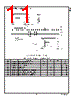
️· READ Transaction (i80 CPU Interface):
- Master-Side Timing:
■ T1: Set Up Time (A/D, RD*): 3.5 cycles
■ T2: Hold Time (A/D, RD*): 2.5 cycles
■ T3: Master Latency: 7 cycles
■ T4: Slave Latency: 4 cycles
- Slave-Side Timing:
■ T5: Read* Delay: 1 cycle
■ T6: Read Low Pulse Width: 6 cycles
■ T7: Data Set Up Time: 5 cycles
■ T8: Data Hold Time: 5 cycles
■ T9: Slave Read Latency: 4 cycles
■ T10: MST Read Latency and INTR Delay: 14 cycles
■ T11: Data Delay: 13-41 cycles
■ T12: Data Valid after Strobe: 1-7.5 cycles
■ T13: RD* active pulse width: >50 cycles
■ T14: INTR De-assert: 5 cycles
■ T15: Recovery Time: 5 cycles
■ T16: INTR Response: 0 cycles
3. Important Operational Aspects
️· Slave Output Recreation: The Slave recreates the transaction, but its exact timing might differ from the Master's input.
️· State Holding: After a WRITE transaction, the Slave's output signals (A/D, DATAn, CS1*) remain in their last state until the next transaction or a power down.
️· IDR Input: The Slave's IDR input determines whether to perform one or two read operations, for consistent behaviour with or without the MPL link. If IDR is High, it performs two read transactions, increasing the time for the INTR signal to be asserted.
️· INTR Signal: Used to signal the completion of a read transaction and to trigger a second read from the host.
️· Clock Rate Adjustment: If the Slave output timing is too fast, a slower MC rate (lower input CLK frequency) should be used.
4. Figure References
️· Figure 11: Illustrates a WRITE transaction.
️· Figure 13: Shows Slave output timing with IDR = High.
Key Takeaway: The text provides detailed timing specifications and operational considerations for ensuring a reliable and compatible interface between the Master and Slave devices, particularly for display-related applications.
1. General Overview
️· Purpose: This document describes the timing and operational details of a communication link (likely a serial interface called MPL) designed for connecting a host (Master) to a peripheral (Slave), potentially for display applications.
️· Goal: To ensure compatibility between the Master and Slave devices regarding timing requirements.
️· Key Feature: Dual Read Operation: Enables consistent behavior regardless of MPL link usage.
2. Timing Parameters & Transactions
️· WRITE Transaction (i80 CPU Interface):
- Master-Side Timing:
■ T1: Data Setup before Write* High: 3.5 cycles
■ T2: Data Hold after Write* High: 2.5 cycles
■ T3: Write Cycle Rate: 6 cycles
■ T4: Master Latency: 7 cycles
■ T5: Slave Latency: 5 cycles
- Slave-Side Timing:
■ T6: Data Valid before Write* High-to-Low: 1 cycle
■ T7: WR* Pulse Width (16-bit mode): 3 cycles
■ T8: Data Valid before Write* Low-to-High: 3 cycles
■ T9: Data Valid after Write* Low-to-High: 1 cycle
️· READ Transaction (i80 CPU Interface):
- Master-Side Timing:
■ T1: Set Up Time (A/D, RD*): 3.5 cycles
■ T2: Hold Time (A/D, RD*): 2.5 cycles
■ T3: Master Latency: 7 cycles
■ T4: Slave Latency: 4 cycles
- Slave-Side Timing:
■ T5: Read* Delay: 1 cycle
■ T6: Read Low Pulse Width: 6 cycles
■ T7: Data Set Up Time: 5 cycles
■ T8: Data Hold Time: 5 cycles
■ T9: Slave Read Latency: 4 cycles
■ T10: MST Read Latency and INTR Delay: 14 cycles
■ T11: Data Delay: 13-41 cycles
■ T12: Data Valid after Strobe: 1-7.5 cycles
■ T13: RD* active pulse width: >50 cycles
■ T14: INTR De-assert: 5 cycles
■ T15: Recovery Time: 5 cycles
■ T16: INTR Response: 0 cycles
3. Important Operational Aspects
️· Slave Output Recreation: The Slave recreates the transaction, but its exact timing might differ from the Master's input.
️· State Holding: After a WRITE transaction, the Slave's output signals (A/D, DATAn, CS1*) remain in their last state until the next transaction or a power down.
️· IDR Input: The Slave's IDR input determines whether to perform one or two read operations, for consistent behaviour with or without the MPL link. If IDR is High, it performs two read transactions, increasing the time for the INTR signal to be asserted.
️· INTR Signal: Used to signal the completion of a read transaction and to trigger a second read from the host.
️· Clock Rate Adjustment: If the Slave output timing is too fast, a slower MC rate (lower input CLK frequency) should be used.
4. Figure References
️· Figure 11: Illustrates a WRITE transaction.
️· Figure 13: Shows Slave output timing with IDR = High.
Key Takeaway: The text provides detailed timing specifications and operational considerations for ensuring a reliable and compatible interface between the Master and Slave devices, particularly for display-related applications.
| Part No. | LM2507 |
| Manufacturer | NSC |
| Size | 977 Kbytes |
| Pages | 22 pages |
| Description | Low Power Mobile Pixel Link (MPL) Level 0, 16-bit CPU Display interface Serializer and Deserializer |
| ALLDATASHEETはお客様のビジネスに役立ちますか? [ DONATE ] |
Alldatasheetは | 広告 | お問い合わせ | プライバシーポリシー | データシートへのリンク | リンク交換 | メーカーリスト All Rights Reserved©Alldatasheet.com |
| Russian : Alldatasheetru.com | Korean : Alldatasheet.co.kr | Spanish : Alldatasheet.es | French : Alldatasheet.fr | Italian : Alldatasheetit.com Portuguese : Alldatasheetpt.com | Polish : Alldatasheet.pl | Vietnamese : Alldatasheet.vn Indian : Alldatasheet.in | Mexican : Alldatasheet.com.mx | British : Alldatasheet.co.uk | New Zealand : Alldatasheet.co.nz |
|
Family Site : ic2ic.com |
icmetro.com |
 Japanese ▼
  English
 Chinese
 German
 Russian
 Korean
 Spanish
 French
 Italian
 Portuguese
 Polish
 Vietnamese
 Indian
 Mexican
 British
 New Zealand