|
データシートサーチシステム |
|
|
データシートサーチシステム |
|
LM2507 データシート(PDF) 6 Page - National Semiconductor (TI) |
|
|
|
|||||||||||||||||||||||||||||
LM2507 データシート(HTML) 6 Page - National Semiconductor (TI) |
|
|
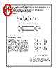
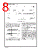
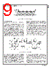
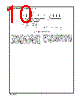
6 / 22 page  Recommended Input Timing Requirements (Continued) Note 5: Total Supply Current Conditions: CPU Mode, worse case data pattern, 19.2MHz CLK, DES CL = 15pF, TYP – VDDIO =VDDA =VDDcore = 1.8V, MAX – VDDIO = 3.0V and VDDA =VDDcore = 2.0V. Note 6: Applies to WR* and RD* outputs only.. Note 7: Maximum transition time is a function of clock rate and should be less than 30% of the clock period to preserve signal quality. Note 8: Guaranteed functionally by the IDDZ parameter. See also Figure 7. Note 9: This is a functional parameter and is guaranteed by design or characterization. Timing Diagrams Functional Description BUS OVERVIEW The LM2507 is a dual link MST/SLV configurable part that supports a 8, 9 or 16-bit CPU (i80 style) interface. The MPL physical layer is purpose-built for an extremely low power and low EMI data transmission while requiring the fewest number of signal lines. No external line components are required, as termination is provided internal to the MPL receiver. A maximum raw throughput of 320 Mbps (raw) is possible with this chipset. When the protocol overhead is taken into account, a maximum data throughput of 240 Mbps is possible. The MPL interface is designed for use with common 50 Ω to 100Ω lines using standard materials and connectors. Lines may be microstrip or stripline construction. Total length of the interconnect is expected to be less than 20cm. SERIAL BUS TIMING Data valid is relative to both edges for a CPU WRITE as shown in Figure 4. Data valid is specified as: Data Valid before Clock, Data Valid after Clock, and Skew between data lines should be less than 500ps. 20186016 FIGURE 1. Serial Data Valid — SLV Input Set and Hold Time 20186018 FIGURE 2. SLV Output Rise and Fall Time 20186002 FIGURE 3. MPL Point-to-Point Bus www.national.com 6 |
|
|
リンク URL |
| ALLDATASHEETはお客様のビジネスに役立ちますか? [ DONATE ] |
Alldatasheetは | 広告 | お問い合わせ | プライバシーポリシー | データシートへのリンク | リンク交換 | メーカーリスト All Rights Reserved©Alldatasheet.com |
| Russian : Alldatasheetru.com | Korean : Alldatasheet.co.kr | Spanish : Alldatasheet.es | French : Alldatasheet.fr | Italian : Alldatasheetit.com Portuguese : Alldatasheetpt.com | Polish : Alldatasheet.pl | Vietnamese : Alldatasheet.vn Indian : Alldatasheet.in | Mexican : Alldatasheet.com.mx | British : Alldatasheet.co.uk | New Zealand : Alldatasheet.co.nz |
|
Family Site : ic2ic.com |
icmetro.com |
 Japanese ▼
 English
 Chinese
 German
 Japanese
 Russian
 Korean
 Spanish
 French
 Italian
 Portuguese
 Polish
 Vietnamese
 Indian
 Mexican
 British
 New Zealand