|
データシートサーチシステム |
|
|
データシートサーチシステム |
|
LM2507 データシート(PDF) 17 Page - National Semiconductor (TI) |
|
|
|
|||||||||||||||||||||||||||||
LM2507 データシート(HTML) 17 Page - National Semiconductor (TI) |
|
|
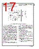
17 / 22 page  Application Information (Continued) Power and Ground - Bumped Package Power and ground bump assignments are shown in Figure 17. The nine center balls must be connected ground on the PCB. See also, National’s Application Note AN-1126, Ball Grid Array, for information on land pattern recommendations and escape routing guidelines. FLEX CIRCUIT RECOMMENDATIONS The three MPL lines should generally run together to mini- mize any trace length differences (skew). For impedance control and also noise isolation (crosstalk), guard ground traces are recommended in between the signals. Commonly a Ground-Signal-Ground (GSGSGSG) layout is used. Lo- cate fast edge rate and large swing signals further away to also minimize any coupling (unwanted crosstalk). In a stacked flex interconnect, crosstalk also needs to be taken into account in the above and below layers (vertical direc- tion). To minimize any coupling locate MPL traces next to a ground layer. Power rails also tend to generate less noise than LVCMOS so they are also good candidates for use as isolation and separation. The interconnect from the Master to the Slave typically acts like a transmission line. Thus impedance control and ground returns are an important part of system design. Impedance should be in the 50 to 100 Ohm nominal range for the LM2507. Testing has been done with cables ranging from 40 to 110 Ohms without error (BER Testing). To obtain the impedance, adjacent grounds are typically required ( 1 layer flex), or a ground shield / layer. Total interconnect length is intended to be in the 20cm range, however 30cm is possible at lower data rates. Skew should be less than 500ps to maximize timing margins. GROUNDING While the LM2507 employs three separate types of ground pins, these are intended to be connected together to a common ground plane. The separate ground pins help to isolate switching currents from different sections of the inte- grated circuit (IC). Also required is a nearby signal return (ground) for the MPL signals. These should be provided next to the MPL signals, as that will create the smallest current loop area. The grounds are also useful for noise isolation and impedance control. PCB RECOMMENDATIONS General guidelines for the PCB design: • Floor plan, locate MPL Master near the connector to limit chance of cross talk to high speed serial signals. • Route serial traces together, minimize the number of layer changes to reduce loading. • Use ground lines are guards to minimize any noise cou- pling (guarantees distance). • Avoid parallel runs with fast edge, large LVCMOS swings. • Also use a GSGSG pinout in connectors (Board to Board or ZIF). • Slave device - follow similar guidelines. • Bypass the device with MLC surface mount devices and thinly separated power and ground planes with low induc- tance feeds. • High current returns should have a separate path with a width proportional to the amount of current carried to minimize any resulting IR effects. 20186021 FIGURE 17. LM2507 PWR (V DD) and GND (VSS) Bumps (TOP VIEW) www.national.com 17 |
|
|
リンク URL |
| ALLDATASHEETはお客様のビジネスに役立ちますか? [ DONATE ] |
Alldatasheetは | 広告 | お問い合わせ | プライバシーポリシー | データシートへのリンク | リンク交換 | メーカーリスト All Rights Reserved©Alldatasheet.com |
| Russian : Alldatasheetru.com | Korean : Alldatasheet.co.kr | Spanish : Alldatasheet.es | French : Alldatasheet.fr | Italian : Alldatasheetit.com Portuguese : Alldatasheetpt.com | Polish : Alldatasheet.pl | Vietnamese : Alldatasheet.vn Indian : Alldatasheet.in | Mexican : Alldatasheet.com.mx | British : Alldatasheet.co.uk | New Zealand : Alldatasheet.co.nz |
|
Family Site : ic2ic.com |
icmetro.com |
 Japanese ▼
 English
 Chinese
 German
 Japanese
 Russian
 Korean
 Spanish
 French
 Italian
 Portuguese
 Polish
 Vietnamese
 Indian
 Mexican
 British
 New Zealand