|
データシートサーチシステム |
|
|
データシートサーチシステム |
|
LM2507 データシート(PDF) 7 Page - National Semiconductor (TI) |
|
|
|
|||||||||||||||||||||||||||||
LM2507 データシート(HTML) 7 Page - National Semiconductor (TI) |
|
|
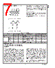
7 / 22 page  Functional Description (Continued) Data is strobed out on the rising edge by the Slave for a CPU READ as shown in Figure 5. The Master monitors for the start bit transition (High to Low) and selects the best strobe to sample the incoming data on. This is done to account for the round trip delay of the interconnect and application data rate. SERIAL BUS PHASES There are four bus phases on the MPL serial bus. These are determined by the state of the MC and MD lines. The MPL bus phases are shown in Table 1. The LM2507 supports MPL Level 0 Enhanced Protocol with a Class 0 PHY. TABLE 1. Link Phases Name MC State MDn State Phase Description Pre-Phase Post-Phase OFF (O) 0 0 Link is Off A, I or LU LU IDLE (I) A H Data is Static (High) A or LU A or O ACTIVE(A) Data Out WRITE A X Data Out (Write) — includes command, Data Out Phases LU, A, or I A, I, or O Data In READ A X Data In (Read) — includes command, TA’, Data In, and TA” phases LU, A, or I A, I, or O LINK-UP (LU) H - Master initiated Link-Up O A, I, or O Notes on MC/MD Line State: 0 = no current (off) L = Logic Low — The higher level of current on the MC and MD lines H = Logic High — The lower level of current on the MC and MD lines X = Low or High A = Active Clock SERIAL BUS START UP TIMING In the Serial Bus OFF phase, Master transmitters for MD0, MD1 and MC are turned off such that zero current flows over the MPL lines. In addition, both the Master and the Slave are internally held in a low power state. When the PD* input pins are de-asserted (driven High) the Master enables its PLL and waits for enough time to pass for its PLL to lock. After the Master’s PLL is locked (t0 = 4,096 CLK Cycles), the Master will perform an MPL start up sequence. The Slave will also power up and await the start up sequence from the Master. The MPL start up sequence gives the Slave an opportunity to optimize the current sources in its transceiver to maximize noise margins. The Master begins the sequence by driving the MC line logically Low for 180 MC cycles (t1). At this point, the Slave’s transceiver samples the MC current flow and adjusts itself to interpret that amount of current as a logical Low. Next the Master drives the MC line logically HIGH for 180 MC cycles (t2). The optimized current configuration is held as long as the MPL remains active. Next, the Master drives both the MC and the MD lines to a logical Low for another 180 MC cycles (t3), after which it begins to toggle the MC line at a rate determined by its PLL setting. The Master will continue to toggle the MC line as long as its PD* pin remains de-asserted (High). At this point the MPL bus may remain in IDLE phase, enter the ACTIVE phase or return to the OFF phase. Active data will occur at the Slave output latency delays (Master + line + Slave) after the data is applied to the Master input. A possible start point is shown by the “C” in Figure 6. In the Figure 6 example, an IDLE bus phase is shown until point C, after which the bus is active and the High start bit on MD initiates the transfer of information. 20186003 FIGURE 4. Dual Link Timing (WRITE) 20186004 FIGURE 5. Dual Link Timing (READ) www.national.com 7 |
|
|
リンク URL |
| ALLDATASHEETはお客様のビジネスに役立ちますか? [ DONATE ] |
Alldatasheetは | 広告 | お問い合わせ | プライバシーポリシー | データシートへのリンク | リンク交換 | メーカーリスト All Rights Reserved©Alldatasheet.com |
| Russian : Alldatasheetru.com | Korean : Alldatasheet.co.kr | Spanish : Alldatasheet.es | French : Alldatasheet.fr | Italian : Alldatasheetit.com Portuguese : Alldatasheetpt.com | Polish : Alldatasheet.pl | Vietnamese : Alldatasheet.vn Indian : Alldatasheet.in | Mexican : Alldatasheet.com.mx | British : Alldatasheet.co.uk | New Zealand : Alldatasheet.co.nz |
|
Family Site : ic2ic.com |
icmetro.com |
 Japanese ▼
 English
 Chinese
 German
 Japanese
 Russian
 Korean
 Spanish
 French
 Italian
 Portuguese
 Polish
 Vietnamese
 Indian
 Mexican
 British
 New Zealand