|
データシートサーチシステム |
|
|
データシートサーチシステム |
|
LM2507 データシート(PDF) 14 Page - National Semiconductor (TI) |
|
|
|
|||||||||||||||||||||||||||||
LM2507 データシート(HTML) 14 Page - National Semiconductor (TI) |
|
|
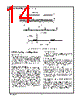
14 / 22 page  Functional Description (Continued) LM2507 Features and Operation POWER SUPPLIES The V DDcore and VDDA (MPL and PLL) must be connected to the same potential between 1.74V and 2.0V. V DDIO powers the logic interface and may be powered between 1.74 and 3.0V to be compatible with a wide range of host and target devices. On this device, V DDIO must be powered up be- fore V DDcore/VDDA for proper device configuration/ startup. BYPASS RECOMMENDATIONS Bypass capacitors should be placed near the power supply pins of the device. Use high frequency ceramic (surface mount recommended) 0.1 µF capacitors. A 2.2 to 4.7 µF Tantalum capacitor is recommended near the Master V DDA pin for PLL bypass. A 2.2 to 4.7 µF Tantalum capacitor is recommended near the Slave V DDA pin for MPL bypass. Connect bypass capacitors with wide traces and use dual or larger via to reduce resistance and inductance of the feeds. Utilizing a thin spacing between power and ground planes will provide good high frequency bypass above the fre- quency range where most typical surface mount capacitors are less effective. To gain the maximum benefit from this, low inductance feed points are important. Also, adjacent signal layers can be filled to create additional capacitance. Mini- mize loops in the ground returns also for improved signal fidelity and lowest emissions. UNUSED/OPEN PINS Unused inputs must be tied to the proper input level — do not float them. Unused outputs should be left open to mini- mize power dissipation. PHASE-LOCKED LOOP When the LM2507 is configured as a CPU Master, a PLL is enabled to generate the serial link clock. The Phase-locked loop system generates the serial data clock at 4X of the input clock. The MC rate is limited between 12MHz and 80MHz which corresponds to an input CLK of 3 to 20MHz. MASTER(SER)/SLAVE(DES) SELECTION The M/S* pin is used to configure the device as either a Master or Slave device. When the M/S* pin is a Logic High, the Master / Serializer configuration is selected. The Driver block is enabled for the MC line, and the MD lines. When the M/S* pin is a Logic Low, the Slave / Deserializer configura- tion is selected. The Receiver block is enabled for the MC line, and the MD lines. POWER DOWN/OFF CONFIGURATION / OPTIONS AND CLOCK STOP Power Up Operation - Upon the application of power to the LM2507, devices configured for Slave activate all outputs. Outputs are held in deasserted states, with all zeros on the data busses until valid data is received from the Master device. If PD* is asserted (Low) prior to the application of power, then the part remains in its power down state. 20186028 FIGURE 14. Two WRITE Timing – Master IN vs. Slave OUT www.national.com 14 |
|
|
リンク URL |
| ALLDATASHEETはお客様のビジネスに役立ちますか? [ DONATE ] |
Alldatasheetは | 広告 | お問い合わせ | プライバシーポリシー | データシートへのリンク | リンク交換 | メーカーリスト All Rights Reserved©Alldatasheet.com |
| Russian : Alldatasheetru.com | Korean : Alldatasheet.co.kr | Spanish : Alldatasheet.es | French : Alldatasheet.fr | Italian : Alldatasheetit.com Portuguese : Alldatasheetpt.com | Polish : Alldatasheet.pl | Vietnamese : Alldatasheet.vn Indian : Alldatasheet.in | Mexican : Alldatasheet.com.mx | British : Alldatasheet.co.uk | New Zealand : Alldatasheet.co.nz |
|
Family Site : ic2ic.com |
icmetro.com |
 Japanese ▼
 English
 Chinese
 German
 Japanese
 Russian
 Korean
 Spanish
 French
 Italian
 Portuguese
 Polish
 Vietnamese
 Indian
 Mexican
 British
 New Zealand