|
データシートサーチシステム |
|
|
データシートサーチシステム |
|
L99DZ81EP データシート(PDF) 9 Page - STMicroelectronics |
|
|
|||||||||||||||||||||||||||||
L99DZ81EP データシート(HTML) 9 Page - STMicroelectronics |
|
|
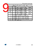
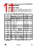
9 / 62 page  DocID023145 Rev 2 9/62 L99DZ81EP Block diagram and pin description 61 13 GH2 GH2: gate driver for power MOS high side switch in half-bridge 2. 14 SH2 SH2: source of high-side switch in half-bridge 2. 15 GL2 GL2: gate driver for power MOS low side switch in half-bridge 2. 16 SL2 SL2: source of low side switch in half-bridge 2. 64 GH1 GH1: gate driver for power MOS high side switch in half-bridge 1. 1 SH1 SH1: source of high-side switch in half-bridge 1. 4 GL1 GL1: gate driver for power MOS low side switch in half-bridge 1. 5 SL1 SL1: source of low side switch in half-bridge 1. 7 CP1P CP1P: charge pump pin for capacitor 1, positive side. 8 CP1M CP1M: charge pump pin for capacitor 1, negative side. 9 CP2P CP2P: charge pump pin for capacitor 2, positive side. 10 CP2M CP2M: charge pump pin for capacitor 2, negative side. 6 CP CP: charge pump output. Table 2. Pin definitions and functions (continued) Pin Symbol Function |
|
リンク URL |
| ALLDATASHEETはお客様のビジネスに役立ちますか? [ DONATE ] |
Alldatasheetは | 広告 | お問い合わせ | プライバシーポリシー | データシートへのリンク | リンク交換 | メーカーリスト All Rights Reserved©Alldatasheet.com |
| Russian : Alldatasheetru.com | Korean : Alldatasheet.co.kr | Spanish : Alldatasheet.es | French : Alldatasheet.fr | Italian : Alldatasheetit.com Portuguese : Alldatasheetpt.com | Polish : Alldatasheet.pl | Vietnamese : Alldatasheet.vn Indian : Alldatasheet.in | Mexican : Alldatasheet.com.mx | British : Alldatasheet.co.uk | New Zealand : Alldatasheet.co.nz |
|
Family Site : ic2ic.com |
icmetro.com |
 Japanese ▼
 English
 Chinese
 German
 Japanese
 Russian
 Korean
 Spanish
 French
 Italian
 Portuguese
 Polish
 Vietnamese
 Indian
 Mexican
 British
 New Zealand