|
データシートサーチシステム |
|
|
データシートサーチシステム |
|
ADRF6655ACPZ-R7 データシート(PDF) 8 Page - Analog Devices |
|
|
|||||||||||||||||||||||||||||
ADRF6655ACPZ-R7 データシート(HTML) 8 Page - Analog Devices |
|
|
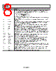
8 / 44 page  ADRF6655 Rev. 0 | Page 8 of 44 Pin No. Mnemonic Description 5 RSET Charge Pump Current. The nominal charge pump current can be set to either 250 μA, 500 μA, 750 μA, or 1 mA using DB10 and DB11 of Register 4 and by setting DB18 to 0 (internal reference current). In this mode, no external RSET is required. If DB18 is set to 1, the four nominal charge pump currents (INOMINAL) can be externally tweaked according to [] 8 . 37 250 4 . 217 , − ⎥⎦ ⎤ ⎢⎣ ⎡ × = Ω BASE CP I RSET where ICP, BASE is the base charge pump current in μA. For further details on the charge pump current,see the Register 4—Charge Pump, PFD, and Reference Path Control section. 6 REFIN Reference Input. Nominal input level is 1 V p-p. Input range is 10 MHz to 160 MHz. This pin must be ac-coupled. 8 MUXOUT Multiplexer Output. This output allows either a digital lock detect, a voltage proportional to temperature, or a buffered, frequency-scaled reference signal to be accessed externally. The output is selected by programming the appropriate bits in Register 4. 9 DECL2 Decoupling Node for 2.5 V LDO. Pin should be decoupled with 100 pF, 0.1 μF, and 10 μF capacitors located close to the pin. 10 VCC2 Power Supply for Internal 2.5 V LDO. The power supply voltage range is 4.75 V to 5.25 V. Supply pin should be decoupled with 100 pF and 0.1 μF capacitors located close to the pin. 12 DATA Serial Data Input. The serial data input is loaded MSB first with the three LSBs being the control bits. 13 CLK Serial Clock Input. This serial clock input is used to clock in the serial data to the registers. The data is latched into the 24-bit shift register on the CLK rising edge. Maximum clock frequency is 20 MHz. 14 LE Load Enable. When the LE input pin goes high, the data stored in the shift registers is loaded into one of the six registers, the relevant latch being selected by the first three control bits of the 24-bit word. 16, 32, 33 NC No Connection. 17, 34 VCCLO Power Supply for LO Path. The power supply voltage range is 4.75 V to 5.25 V. Supply pin should be decoupled with 100 pF and 0.1 μF capacitors located close to the pin. 18,19 OUTN, OUTP Mixer IF Outputs. These pins should be pulled to VCC with RF chokes. 22 VCCV2I Power Supply for Voltage to Current Input Stage. The power supply voltage range is 4.75 V to 5.25 V. Supply pin should be decoupled with 100 pF and 0.1 μF capacitors located close to the pin. 25, 26 INN, INP Mixer RF Inputs. Differential RF Inputs. Internally matched to 50 Ω. This pin must be ac-coupled. 27 VCCMIX Power Supply for Mixer. The power supply voltage range is 4.75 V to 5.25 V. Supply pin should be decoupled with 100 pF and 0.1 μF capacitors located close to the pin. 29 IP3SET Connect Resistor to VCC to Adjust IP3. 37, 38 LON, LOP Local Oscillator Input/Output. The internally generated 1 × fLO is available on these pins. When internal LO generation is disabled, an external 2 × fLO or 3 × fLO (depending on divider selection) can be applied to these pins. This pin must be ac-coupled. 39 VTUNE VCO Control Voltage Input. This pin is driven by the output of the loop filter. Nominal input voltage range on this pin is 1 V to 2.8 V. 40 DECL3 Decoupling Node for VCO LDO. Connect a 100 pF capacitor and a 10 μF capacitor between this pin and ground. EPAD (EP) The exposed paddle should be soldered to a low impedance ground plane. |
|
リンク URL |
| ALLDATASHEETはお客様のビジネスに役立ちますか? [ DONATE ] |
Alldatasheetは | 広告 | お問い合わせ | プライバシーポリシー | データシートへのリンク | リンク交換 | メーカーリスト All Rights Reserved©Alldatasheet.com |
| Russian : Alldatasheetru.com | Korean : Alldatasheet.co.kr | Spanish : Alldatasheet.es | French : Alldatasheet.fr | Italian : Alldatasheetit.com Portuguese : Alldatasheetpt.com | Polish : Alldatasheet.pl | Vietnamese : Alldatasheet.vn Indian : Alldatasheet.in | Mexican : Alldatasheet.com.mx | British : Alldatasheet.co.uk | New Zealand : Alldatasheet.co.nz |
|
Family Site : ic2ic.com |
icmetro.com |
 Japanese ▼
 English
 Chinese
 German
 Japanese
 Russian
 Korean
 Spanish
 French
 Italian
 Portuguese
 Polish
 Vietnamese
 Indian
 Mexican
 British
 New Zealand