|
データシートサーチシステム |
|
|
データシートサーチシステム |
|
L9908 データシート(PDF) 138 Page - STMicroelectronics |
|
|
|||||||||||||||||||||||||||||
L9908 データシート(HTML) 138 Page - STMicroelectronics |
|
|
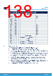
138 / 152 page  Component Min Typ Max Unit Minimum requirement Comment 12 V systems 24 V systems 48 V systems RDC - 4 - mΩ WSL10204L000FEA - REN_BR - 100 - Ω - Optional RFS_FLAG - 100 - Ω - Optional RGHS1n - 47 - Ω - - RGHS2n - 100 - kΩ - - RGLS1n - 47 - Ω - - RGLS2n - 100 - kΩ - - RINHn - 100 - Ω - Optional RINLn - 100 - Ω - Optional RNCS - 100 - Ω - Optional RNDIS - 100 - Ω - Optional RSCLK - 100 - Ω - Optional RSDI - 100 - Ω - Optional RSDO - 100 - Ω - Optional RSHUNTn - 4 - mΩ WSL10204L000FEA - TBR1 - - - - STL225N6F7AG STH275N8F7 - TBR2 - - - - BCP56-16 - TVBP1 - - - - BCP56-16 - THSn - - - - STL225N6F7AG STD105N10F7AG - TLSn - - - - STL225N6F7AG STD105N10F7AG - 6.4 Layout guidelines The following layout guidelines apply to any of the above shown application circuits. • Three separated bulk capacitors CHB1 should be used - one per half bridge. • Three separated ceramic capacitors CHB2 should be used - one per half bridge. • Each of the 3 bulk capacitors CHB1 and each of the 3 ceramic capacitors CHB2 should be assigned to one of the half bridges and should be placed very close to it. • The components within one half bridge should be placed close to each other to reduce stray inductance to a minimum: high-side MOSFET, low-side MOSFET, bulk capacitor CHB1, ceramic capacitor CHB2 and the shunt resistor RSHUNT form a loop that should be as small and tight as possible. The traces should be short and wide. • The three half bridges can be separated; however, when there is one common GND referenced shunt resistor (RDC) for the three half bridges the sources of all low-side MOSFETs should be close to each other and close to the common shunt resistor. • Additional R-C snubber circuits can be placed to attenuate/suppress oscillations during switching of the MOSFETs, there may be one or two snubber circuits per half bridge and components must be low inductive in terms of routing and packaging (ceramic capacitors). • The exposed pad on the backside of the package shall be connected to GND. L9908 Application circuit DS13546 - Rev 5 page 138/152 |
|
リンク URL |
| ALLDATASHEETはお客様のビジネスに役立ちますか? [ DONATE ] |
Alldatasheetは | 広告 | お問い合わせ | プライバシーポリシー | データシートへのリンク | リンク交換 | メーカーリスト All Rights Reserved©Alldatasheet.com |
| Russian : Alldatasheetru.com | Korean : Alldatasheet.co.kr | Spanish : Alldatasheet.es | French : Alldatasheet.fr | Italian : Alldatasheetit.com Portuguese : Alldatasheetpt.com | Polish : Alldatasheet.pl | Vietnamese : Alldatasheet.vn Indian : Alldatasheet.in | Mexican : Alldatasheet.com.mx | British : Alldatasheet.co.uk | New Zealand : Alldatasheet.co.nz |
|
Family Site : ic2ic.com |
icmetro.com |
 Japanese ▼
 English
 Chinese
 German
 Japanese
 Russian
 Korean
 Spanish
 French
 Italian
 Portuguese
 Polish
 Vietnamese
 Indian
 Mexican
 British
 New Zealand