|
データシートサーチシステム |
|
|
データシートサーチシステム |
|
MCP3901A2T-I/SS データシート(PDF) 44 Page - Microchip Technology |
|
|
|||||||||||||||||||||||||||||
MCP3901A2T-I/SS データシート(HTML) 44 Page - Microchip Technology |
|
|
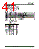
44 / 60 page  MCP3901 DS22192A-page 44 © 2009 Microchip Technology Inc. 7.3 PHASE Register The PHASE register (PHASE<7:0>) is a 7 bits + sign MSB first two's complement register that indicates how much phase delay there should be between Channel 0 and Channel 1. The reference channel for the delay is channel 1 (typically the voltage channel when used in energy metering applications), i.e. when PHASE register code is positive, Channel 0 is lagging channel 1. When PHASE register code is negative, Channel 0 is leading versus Channel 1. The delay is give by the following formula: EQUATION 7-1: 7.3.1 PHASE RESOLUTION FROM OSR The timing resolution of the phase delay is 1/DMCLK or 1 µs in the default configuration (MCLK=4 MHz). The PHASE register coding depends on the OSR setting: • OSR=256: the delay can go from -128 to +127. PHASE<7> is the sign bit. Phase<6> is the MSB and PHASE<0> the LSB. • OSR=128: the delay can go from -64 to +63. PHASE<6> is the sign bit. Phase<5> is the MSB and PHASE<0> the LSB. • OSR=64: the delay can go from -32 to +31. PHASE<5> is the sign bit. Phase<4> is the MSB and PHASE<0> the LSB. • OSR=32: the delay can go from -16 to +15. PHASE<4> is the sign bit. Phase<3> is the MSB and PHASE<0> the LSB. Delay Phase Register Code DMCLK -------------------------------------------------- = REGISTER 7-3: PHASE REGISTER (PHASE): ADDRESS 0X07 R/W-0 R/W-0 R/W-0 R/W-0 R/W-0 R/W-0 R/W-0 R/W-0 PHASE<7> PHASE<6> PHASE<5> PHASE<4> PHASE<3> PHASE<2> PHASE<1> PHASE<0> bit 7 bit 0 Legend: R = Readable bit W = Writable bit U = Unimplemented bit, read as ‘0’ -n = Value at POR ‘1’ = Bit is set ‘0’ = Bit is cleared x = Bit is unknown bit 7:0 CH0 relative to CH1 phase delay Delay = PHASE Register two’s complement code / DMCLK (Default PHASE=0) |
|
リンク URL |
| ALLDATASHEETはお客様のビジネスに役立ちますか? [ DONATE ] |
Alldatasheetは | 広告 | お問い合わせ | プライバシーポリシー | データシートへのリンク | リンク交換 | メーカーリスト All Rights Reserved©Alldatasheet.com |
| Russian : Alldatasheetru.com | Korean : Alldatasheet.co.kr | Spanish : Alldatasheet.es | French : Alldatasheet.fr | Italian : Alldatasheetit.com Portuguese : Alldatasheetpt.com | Polish : Alldatasheet.pl | Vietnamese : Alldatasheet.vn Indian : Alldatasheet.in | Mexican : Alldatasheet.com.mx | British : Alldatasheet.co.uk | New Zealand : Alldatasheet.co.nz |
|
Family Site : ic2ic.com |
icmetro.com |
 Japanese ▼
 English
 Chinese
 German
 Japanese
 Russian
 Korean
 Spanish
 French
 Italian
 Portuguese
 Polish
 Vietnamese
 Indian
 Mexican
 British
 New Zealand