|
データシートサーチシステム |
|
|
データシートサーチシステム |
|
TX58TEGXDDKTAX0 データシート(PDF) 12 Page - Toshiba Semiconductor |
|
|
|||||||||||||||||||||||||||||
TX58TEGXDDKTAX0 データシート(HTML) 12 Page - Toshiba Semiconductor |
|
|
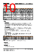
12 / 121 page  TOSHIBA CONFIDENTIAL Tx58TEGxDDKTAx0 TENTATIVE 2013-07-10C 11 TC58TEG6DDKTA00 / TC58TEG6DDKTAI0 TH58TEG7DDKTA20 / TH58TEG7DDKTAK0 TH58TEG8DDKTA20 / TH58TEG8DDKTAK0 2. PHYSICAL INTERFACE 2.1. Pin Descriptions Table 3 Pin Descriptions SDR Toggle DDR1.0 Pin Function DQ[7:0] DQ[7:0] DATA INPUTS/OUTPUTS The DQ pins are used to input command, address and data and to output data during read operations. The DQ pins float to high-z when the chip is deselected or when the outputs are disabled. CLE CLE COMMAND LATCH ENABLE The CLE input controls the activating path for commands sent to the command register. When active high, commands are latched into the command register through the DQ ports on the rising edge of the WE signal. ALE ALE ADDRESS LATCH ENABLE The ALE input controls the activating path for address to the internal address registers. Addresses are latched on the rising edge of WE with ALE high. CE CE CHIP ENABLE The CE input is the device selection control. When the device is in the Busy state, CE high is ignored, and the device does not return to standby mode in program or erase operation. RE RE READ ENABLE The RE input is the serial data-out control, and when active, drives the data onto the DQ bus. Data is valid after tDQSRE of rising edge & falling edge of RE , which also increments the internal column address counter by each one. WE WE WRITE ENABLE The WE input controls writes to the DQ port. Commands, addresses are latched on the rising edge of the WE pulse. WP WP WRITE PROTECT The WP pin provides inadvertent program/erase protection during power transitions. The internal high voltage generator is reset when the WP pin is active low. R/ B R/ B READY/BUSY OUTPUT The R/ B output indicates the status of the device operation. When low, it indicates that a program, erase or random read operation is in process and returns to high state upon completion. It is an open drain output and does not float to high-z condition when the chip is deselected or when outputs are disabled. - DQS DATA STROBE Output with read data, input with write data. Edge-aligned with read data, centered in write data. Vcc Vcc POWER VCC is the power supply for device. VccQ VccQ DQ POWER The VccQ is the power supply for input and/or output signals. Vss Vss GROUND VssQ VssQ DQ GROUND The VssQ is the power supply ground VPP VPP External VPP The VPP signal is an optional external high voltage power supply to the device. This high voltage power supply may be used to enhance Erase and Program operations (e.g., improved power efficiency). NC NC No connection NCs are not internally connected. They can be driven or left unconnected. NU NU Not use NUs must be left unconnected. NOTE: 1) Connect all Vcc and Vss pins of each device to common power supply outputs. 2) Do not leave all Vcc, VccQ, Vss and VssQ disconnected. |
|
リンク URL |
| ALLDATASHEETはお客様のビジネスに役立ちますか? [ DONATE ] |
Alldatasheetは | 広告 | お問い合わせ | プライバシーポリシー | データシートへのリンク | リンク交換 | メーカーリスト All Rights Reserved©Alldatasheet.com |
| Russian : Alldatasheetru.com | Korean : Alldatasheet.co.kr | Spanish : Alldatasheet.es | French : Alldatasheet.fr | Italian : Alldatasheetit.com Portuguese : Alldatasheetpt.com | Polish : Alldatasheet.pl | Vietnamese : Alldatasheet.vn Indian : Alldatasheet.in | Mexican : Alldatasheet.com.mx | British : Alldatasheet.co.uk | New Zealand : Alldatasheet.co.nz |
|
Family Site : ic2ic.com |
icmetro.com |
 Japanese ▼
 English
 Chinese
 German
 Japanese
 Russian
 Korean
 Spanish
 French
 Italian
 Portuguese
 Polish
 Vietnamese
 Indian
 Mexican
 British
 New Zealand