|
データシートサーチシステム |
|
|
データシートサーチシステム |
|
MCP6V06T データシート(PDF) 21 Page - Microchip Technology |
|
|
|||||||||||||||||||||||||||||
MCP6V06T データシート(HTML) 21 Page - Microchip Technology |
|
|
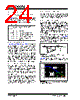
21 / 44 page  © 2008 Microchip Technology Inc. DS22093B-page 21 MCP6V06/7/8 4.0 APPLICATIONS The MCP6V06/7/8 family of auto-zeroed op amps is manufactured using Microchip’s state of the art CMOS process. It is designed for low cost, low power and high precision applications. Its low supply voltage, low quiescent current and wide bandwidth makes the MCP6V06/7/8 ideal for battery-powered applications. 4.1 Overview of Auto-zeroing Operation Figure 4-1 shows a simplified diagram of the MCP6V06/7/8 auto-zeroed op amps. This will be used to explain how the DC voltage errors are reduced in this architecture. FIGURE 4-1: Simplified Auto-zeroed Op Amp Functional Diagram. 4.1.1 BUILDING BLOCKS The Null Amp. and Main Amp. are designed for high gain and accuracy using a differential topology. They have an auxiliary input (bottom left) used for correcting the offset voltages. Both inputs are added together internally. The capacitors at the auxiliary inputs (CFW and CH) hold the corrected values during normal operation. The Output Buffer is designed to drive external loads at the VOUT pin. It also produces a single ended output voltage (VREF is an internal reference voltage). All of these switches are make-before-break in order to minimize glitch-induced errors. They are driven by two clock phases ( φ1 and φ2) that select between normal mode and auto-zeroing mode. The clock is derived from an internal R-C oscillator running at a rate of fOSC1 = 650 kHz. The oscillator’s output is divided down to the desired rate. It is also randomized to minimize (spread) undesired clock tones in the output. The internal POR ensures the part starts up in a known good state. It also provides protection against power supply brown out events. The Chip Select input places the op amp in a low power state when it is high. When it goes low, it powers the op amp at its normal level and starts operation properly. The Digital Control circuitry takes care of all of the housekeeping details of the switching operation. It also takes care of Chip Select and POR events. VIN+ VIN– Main Output VOUT VREF Amp. Buffer NC Null Amp. Null Input φ1 Switches Null Correct φ2 Switches Null Output Switches CH CFW POR Digital Control Oscillator CS Clock Randomization φ1 φ2 |
|
リンク URL |
| ALLDATASHEETはお客様のビジネスに役立ちますか? [ DONATE ] |
Alldatasheetは | 広告 | お問い合わせ | プライバシーポリシー | データシートへのリンク | リンク交換 | メーカーリスト All Rights Reserved©Alldatasheet.com |
| Russian : Alldatasheetru.com | Korean : Alldatasheet.co.kr | Spanish : Alldatasheet.es | French : Alldatasheet.fr | Italian : Alldatasheetit.com Portuguese : Alldatasheetpt.com | Polish : Alldatasheet.pl | Vietnamese : Alldatasheet.vn Indian : Alldatasheet.in | Mexican : Alldatasheet.com.mx | British : Alldatasheet.co.uk | New Zealand : Alldatasheet.co.nz |
|
Family Site : ic2ic.com |
icmetro.com |
 Japanese ▼
 English
 Chinese
 German
 Japanese
 Russian
 Korean
 Spanish
 French
 Italian
 Portuguese
 Polish
 Vietnamese
 Indian
 Mexican
 British
 New Zealand