|
データシートサーチシステム |
|
|
データシートサーチシステム |
|
MCP6V06T データシート(PDF) 26 Page - Microchip Technology |
|
|
|||||||||||||||||||||||||||||
MCP6V06T データシート(HTML) 26 Page - Microchip Technology |
|
|
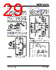
26 / 44 page  MCP6V06/7/8 DS22093B-page 26 © 2008 Microchip Technology Inc. 4.3.9 PCB DESIGN FOR DC PRECISION In order to achieve DC precision on the order of ±1 µV, many physical errors need to be minimized. The design of the Printed Circuit Board (PCB), the wiring, and the thermal environment has a strong impact on the precision achieved. A poor PCB design can easily be more than 100 times worse than the MCP6V06/7/8 op amps minimum and maximum specifications. 4.3.9.1 Thermo-junctions Any time two dissimilar metals are joined together, a temperature dependent voltage appears across the junction (the Seebeck or thermo-junction effect). This effect is used in thermocouples to measure tempera- ture. The following are examples of thermo-junctions on a PCB: • Components (resistors, op amps, …) soldered to a copper pad • Wires mechanically attached to the PCB • Jumpers •Solder joints •PCB vias Typical thermo-junctions have temperature to voltage conversion coefficients of 10 to 100 µV/°C (sometimes higher). There are three basic approaches to minimizing thermo-junction effects: • Minimize thermal gradients • Cancel thermo-junction voltages • Minimize difference in thermal potential between metals 4.3.9.2 Non-inverting and Inverting Amplifier Layout for Thermo-junctions Figure 4-11 shows the recommended non-inverting and inverting gain amplifier circuits on one schematic. Usually, to minimize the input bias current related off- set, R1 is chosen to be R2||R3. The guard traces (with ground vias at the ends) help minimize the thermal gradients. The resistor layout cancels the resistor thermal voltages, assuming the temperature gradient is constant near the resistors: EQUATION 4-2: FIGURE 4-11: PCB Layout and Schematic for Single Non-inverting and Inverting Amplifiers. Note: Changing the orientation of the resistors will usually cause a significant decrease in the cancellation of the thermal voltages. VOUT ≈ VPGP,VM =GND ≈ -VMGM,VP =GND Where: GM =R3/R2, inverting gain magnitude GP =1 + GM, non-inverting gain magnitude VOS is neglected VP R3 VOUT R1 R2 VM U1 MCP6V06 U1 VM VOUT VP R3 R2 R1 |
|
リンク URL |
| ALLDATASHEETはお客様のビジネスに役立ちますか? [ DONATE ] |
Alldatasheetは | 広告 | お問い合わせ | プライバシーポリシー | データシートへのリンク | リンク交換 | メーカーリスト All Rights Reserved©Alldatasheet.com |
| Russian : Alldatasheetru.com | Korean : Alldatasheet.co.kr | Spanish : Alldatasheet.es | French : Alldatasheet.fr | Italian : Alldatasheetit.com Portuguese : Alldatasheetpt.com | Polish : Alldatasheet.pl | Vietnamese : Alldatasheet.vn Indian : Alldatasheet.in | Mexican : Alldatasheet.com.mx | British : Alldatasheet.co.uk | New Zealand : Alldatasheet.co.nz |
|
Family Site : ic2ic.com |
icmetro.com |
 Japanese ▼
 English
 Chinese
 German
 Japanese
 Russian
 Korean
 Spanish
 French
 Italian
 Portuguese
 Polish
 Vietnamese
 Indian
 Mexican
 British
 New Zealand