|
データシートサーチシステム |
|
|
データシートサーチシステム |
|
MCP6V06T データシート(PDF) 29 Page - Microchip Technology |
|
|
|||||||||||||||||||||||||||||
MCP6V06T データシート(HTML) 29 Page - Microchip Technology |
|
|
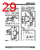
29 / 44 page  © 2008 Microchip Technology Inc. DS22093B-page 29 MCP6V06/7/8 4.4 Typical Applications 4.4.1 WHEATSTONE BRIDGE Many sensors are configured as Wheatstone bridges. Strain gauges and pressure sensors are two common examples. These signals can be small and the common mode noise large. Amplifier designs with high differential gain are desirable. Figure 4-15 shows how to interface to a Wheatstone bridge with a minimum of components. Because the circuit is not symmetric, the ADC input is single ended, and there is a minimum of filtering, the CMRR is good enough for moderate common mode noise. FIGURE 4-15: Simple Design. Figure 4-16 shows a higher performance circuit for Wheatstone bridges. This circuit is symmetric and has high CMRR. Using a differential input to the ADC helps with the CMRR. FIGURE 4-16: High Performance Design. 4.4.2 RTD SENSOR The ratiometric circuit in Figure 4-17 conditions a three wire RTD. It corrects for the sensor’s wiring resistance by subtracting the voltage across the middle RW. The top R1 does not change the output voltage; it balances the op amp inputs. Failure (open) of the RTD is detected by an out-of-range voltage. FIGURE 4-17: RTD Sensor. The voltages at the input of the ADC can be calculated with the following: VDD RR RR 100R 0.01C MCP6V06 ADC VDD 0.2R 0.2R 3k Ω 20 k Ω 1µF 200 Ω 20 k Ω 1µF ADC VDD ½ MCP6V07 ½ MCP6V07 200 Ω 200 Ω 3k Ω 3k Ω 1µF RR RR VDD 10 nF 10 nF 200 Ω R3 100 nF 10 nF R2 R3 100 nF ADC VDD ½ MCP6V07 ½ MCP6V07 2.49 k Ω 2.49 k Ω 10 nF VDD RW RW RW RT RB RRTD R1 R1 1µF 100 Ω 3k Ω 3k Ω 20 k Ω 20 k Ω 100 k Ω 100 k Ω 2.49 k Ω 2.49 k Ω R2 2.55 k Ω 2.55 k Ω V DM G RTD VT V B – () G WVW + = V CM V T V B G RTD 1G W – + ()V W ++ 2 ------------------------------------------------------------------------------ = G RTD 12 R 3 R2 ⁄ ⋅ + = G W G RTD R 3 R1 ⁄ – = Where: VT = Voltage at the top of RRTD VB = Voltage at the bottom of RRTD VW = Voltage across top and middle RW’s VCM = ADC’s common mode input VDM = ADC’s differential mode input |
|
リンク URL |
| ALLDATASHEETはお客様のビジネスに役立ちますか? [ DONATE ] |
Alldatasheetは | 広告 | お問い合わせ | プライバシーポリシー | データシートへのリンク | リンク交換 | メーカーリスト All Rights Reserved©Alldatasheet.com |
| Russian : Alldatasheetru.com | Korean : Alldatasheet.co.kr | Spanish : Alldatasheet.es | French : Alldatasheet.fr | Italian : Alldatasheetit.com Portuguese : Alldatasheetpt.com | Polish : Alldatasheet.pl | Vietnamese : Alldatasheet.vn Indian : Alldatasheet.in | Mexican : Alldatasheet.com.mx | British : Alldatasheet.co.uk | New Zealand : Alldatasheet.co.nz |
|
Family Site : ic2ic.com |
icmetro.com |
 Japanese ▼
 English
 Chinese
 German
 Japanese
 Russian
 Korean
 Spanish
 French
 Italian
 Portuguese
 Polish
 Vietnamese
 Indian
 Mexican
 British
 New Zealand