|
データシートサーチシステム |
|
|
データシートサーチシステム |
|
MCP6V06T データシート(PDF) 25 Page - Microchip Technology |
|
|
|||||||||||||||||||||||||||||
MCP6V06T データシート(HTML) 25 Page - Microchip Technology |
|
|
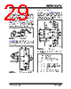
25 / 44 page  © 2008 Microchip Technology Inc. DS22093B-page 25 MCP6V06/7/8 After selecting RISO for your circuit, double check the resulting frequency response peaking and step response overshoot. Modify RISO's value until the response is reasonable. Bench evaluation and simulations with the MCP6V06 SPICE macro model (good for all of the MCP6V06/7/8 op amps) are helpful. 4.3.6 STABILIZING OUTPUT LOADS This family of auto-zeroed op amps has an output impedance (Figure 2-31 and Figure 2-32) that has a double zero when the gain is low. This can cause a large phase shift in feedback networks that have low resistance near the part’s bandwidth. This large phase shift can cause stability problems. Figure 4-8 shows one circuit example that has low resistance near the part’s bandwidth. RF and CF set a pole at 0.16 kHz, so the noise gain (GN) is 1 V/V at the circuit’s bandwidth (roughly 1.3 MHz). The load seen by the op amp’s output at 1.3 MHz is RG||RL (99Ω). This is low enough to be a real concern. FIGURE 4-8: Output Load Issue. To solve this problem, increase the resistive load to at least 3 k Ω. Methods to accomplish this task include: • Increase RG • Remove CF (relocate the filter) • Add a 3 k Ω resistor at the op amp’s output that is not in the signal path; see Figure 4-9 FIGURE 4-9: One Solution To Output Load Issue. 4.3.7 REDUCING UNDESIRED NOISE AND SIGNALS Reduce undesired noise and signals with: • Low bandwidth signal filters: - Minimizes random analog noise - Reduces interfering signals • Good PCB layout techniques: - Minimizes crosstalk - Minimizes parasitic capacitances and induc- tances that interact with fast switching edges • Good power supply design: - Isolation from other parts - Filtering of interference on supply line(s) 4.3.8 SUPPLY BYPASSING AND FILTERING With this family of operational amplifiers, the power supply pin (VDD for single supply) should have a local bypass capacitor (i.e., 0.01 µF to 0.1 µF) within 2 mm of the pin for good high-frequency performance. These parts also need a bulk capacitor (i.e., 1 µF or larger) within 100 mm to provide large, slow currents. This bulk capacitor can be shared with other low noise, analog parts. Additional filtering of high frequency power supply noise (e.g., switched mode power supplies) can be achieved using resistors. The resistors need to be small enough to prevent a large drop in VDD for the op amp, which would cause a reduced output range and possible load-induced power supply noise. The resis- tors also need to be large enough to dissipate little power when VDD is turned on and off quickly. The cir- cuit in Figure 4-10 gives good rejection out to 1 MHz for switched mode power supplies. Smaller resistors and capacitors are a better choice for designs where the power supply is reasonably quiet. FIGURE 4-10: Additional Supply Filtering. MCP6V0X CF 10.0 k Ω RF 100 Ω RG 100 Ω RN VOUT VIN 10.0 k Ω RL 0.1 µF MCP6V0X CF 10.0 k Ω RF 100 Ω RG 100 Ω RN VOUT VIN 10.0 k Ω RL 0.1 µF 3.01 k Ω RX MCP6V0X VS_ANA 143 Ω 143 Ω 100 µF 100 µF 0.1 µF 1/4W 1/10W to other analog parts |
|
リンク URL |
| ALLDATASHEETはお客様のビジネスに役立ちますか? [ DONATE ] |
Alldatasheetは | 広告 | お問い合わせ | プライバシーポリシー | データシートへのリンク | リンク交換 | メーカーリスト All Rights Reserved©Alldatasheet.com |
| Russian : Alldatasheetru.com | Korean : Alldatasheet.co.kr | Spanish : Alldatasheet.es | French : Alldatasheet.fr | Italian : Alldatasheetit.com Portuguese : Alldatasheetpt.com | Polish : Alldatasheet.pl | Vietnamese : Alldatasheet.vn Indian : Alldatasheet.in | Mexican : Alldatasheet.com.mx | British : Alldatasheet.co.uk | New Zealand : Alldatasheet.co.nz |
|
Family Site : ic2ic.com |
icmetro.com |
 Japanese ▼
 English
 Chinese
 German
 Japanese
 Russian
 Korean
 Spanish
 French
 Italian
 Portuguese
 Polish
 Vietnamese
 Indian
 Mexican
 British
 New Zealand