|
データシートサーチシステム |
|
|
データシートサーチシステム |
|
MCP6V06T データシート(PDF) 27 Page - Microchip Technology |
|
|
|||||||||||||||||||||||||||||
MCP6V06T データシート(HTML) 27 Page - Microchip Technology |
|
|
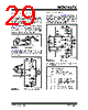
27 / 44 page  © 2008 Microchip Technology Inc. DS22093B-page 27 MCP6V06/7/8 4.3.9.3 Difference Amplifier Layout for Thermo-junctions Figure 4-12 shows the recommended difference ampli- fier circuit. Usually, we choose R1 =R2 and R3 =R4. The guard traces (with ground vias at the ends) help minimize the thermal gradients. The resistor layout cancels the resistor thermal voltages, assuming the temperature gradient is constant near the resistors: EQUATION 4-3: FIGURE 4-12: PCB Layout and Schematic for Single Difference Amplifier. 4.3.9.4 Dual Non-inverting Amplifier Layout for Thermo-junctions The dual op amp amplifiers shown in Figure 4-16 and Figure 4-17 produce a non-inverting difference gain greater than 1, and a common mode gain of 1 .They can use the layout shown in Figure 4-13. The gain set- ting resistors (R2) between the two sides are not com- bined so that the thermal voltages can be canceled. The guard traces (with ground vias at the ends) help minimize the thermal gradients. The resistor layout cancels the resistor thermal voltages, assuming the temperature gradient is constant near the resistors: EQUATION 4-4: FIGURE 4-13: PCB Layout and Schematic for Dual Non-inverting Amplifier. Note: Changing the orientation of the resistors will usually cause a significant decrease in the cancellation of the thermal voltages. VOUT ≈ VREF +(VP –VM)GDM Where: Thermal voltages are approximately equal GDM =R3/R1 =R4/R2, difference gain VOS is neglected VOUT ≈ VREF +(VP –VM)GDM R4 VOUT R2 VM U1 MCP6V06 VP R1 R3 VREF U1 VM VOUT VP R4 R2 R1 R3 VREF Note: Changing the orientation of the resistors will usually cause a significant decrease in the cancellation of the thermal voltages. (VOA –VOB) ≈ (VIA –VIB)GDM (VOA +VOB)/2 ≈ (VIA +VIB)/2 Where: Thermal voltages are approximately equal GDM =1 + R3/R2, differential mode gain GCM = 1, common mode gain VOS is neglected U1 VIB VOA VOB VIA R1 R2 R3 R1 R2 R3 VIB VOB R1 U1 ½MCP6V07 VIA R3 VOA R1 R2 U1 ½MCP6V07 R3 R2 |
|
リンク URL |
| ALLDATASHEETはお客様のビジネスに役立ちますか? [ DONATE ] |
Alldatasheetは | 広告 | お問い合わせ | プライバシーポリシー | データシートへのリンク | リンク交換 | メーカーリスト All Rights Reserved©Alldatasheet.com |
| Russian : Alldatasheetru.com | Korean : Alldatasheet.co.kr | Spanish : Alldatasheet.es | French : Alldatasheet.fr | Italian : Alldatasheetit.com Portuguese : Alldatasheetpt.com | Polish : Alldatasheet.pl | Vietnamese : Alldatasheet.vn Indian : Alldatasheet.in | Mexican : Alldatasheet.com.mx | British : Alldatasheet.co.uk | New Zealand : Alldatasheet.co.nz |
|
Family Site : ic2ic.com |
icmetro.com |
 Japanese ▼
 English
 Chinese
 German
 Japanese
 Russian
 Korean
 Spanish
 French
 Italian
 Portuguese
 Polish
 Vietnamese
 Indian
 Mexican
 British
 New Zealand